Intel
®
IXP42X product line and IXC1100 control plane processors—PCI Controller
Intel
®
IXP42X Product Line of Network Processors and IXC1100 Control Plane Processor
DM September 2006
236 Order Number: 252480-006US
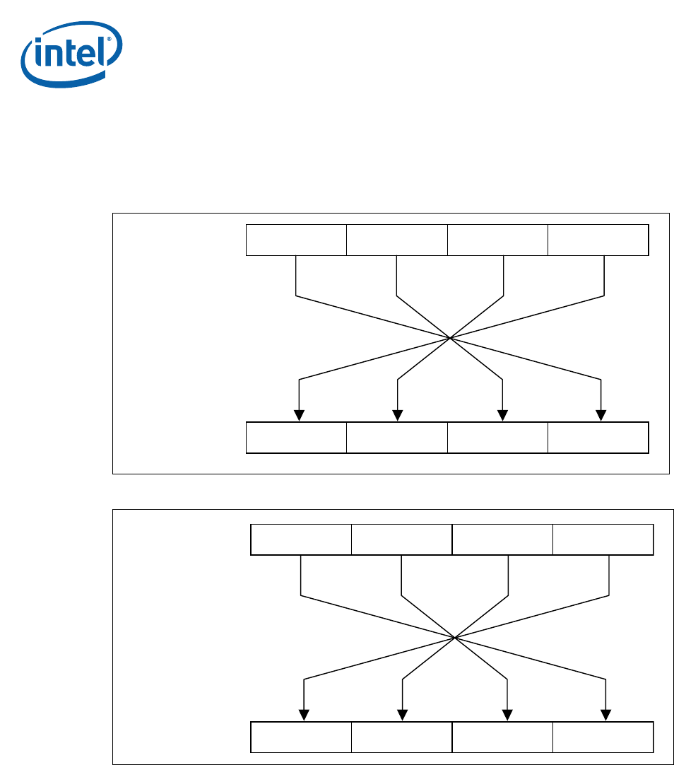
Bit 28 of the Length Register is used to provide a byte swap on the DMA data as
data is transferred from the AHB to the PCI bus or from the PCI Bus to AHB,
depending upon the direction of the DMA transfer. When bit 28 is set to logic 1, a
byte swap will occur on the DMA data. Figure 45 and Figure 46 demonstrates the
DMA transfer byte lane swapping.
The DMA channels share resources with the AHB Master and Target interfaces and
therefore must arbitrate for these resources. AHB-to-PCI DMA transfers use the AHB
Master Interface, the PCI Initiator Request FIFO, and Initiator Transmit FIFO. PCI-to-
AHB DMA transfers use the AHB Master Interface, the PCI Initiator Request FIFO, and
Initiator Receive FIFO. Use of the AHB Master Interface will revolve between the two
DMA channels and PCI requests that appear in the Target Receive FIFO.
While a particular channel is accessing the Initiator Request FIFO, accesses to the PCI
bus coming in to the AHB Target Interface from the AHB will be retried. The access will
be flagged by the hardware to signal the DMA Controller channels that a PCI access is
pending (AHB masters must attempt retried transfers until complete). This enables the
DMA channels to permit the AHB initiated PCI access to go through to the PCI bus.
Figure 45. AHB to PCI DMA Transfer Byte Lane Swapping
Figure 46. PCI to AHB DMA Transfer Byte Lane Swapping
B
y
te 3 B
y
te 0 B
y
te 2 B
y
te 1
B
y
te 0 B
y
te 3 B
y
te 1 B
y
te 2
AHB Dat
a
PCI Dat
a
B
y
te 0 B
y
te 3 B
y
te 1 B
y
te 2
B
y
te 3 B
y
te 0B
y
te 2 B
y
te 1
PCI Dat
a
AHB Dat
a


