Intel
®
IXP42X Product Line of Network Processors and IXC1100 Control Plane Processor
September 2006 DM
Order Number: 252480-006US 233
PCI Controller—Intel
®
IXP42X product line and IXC1100 control plane processors
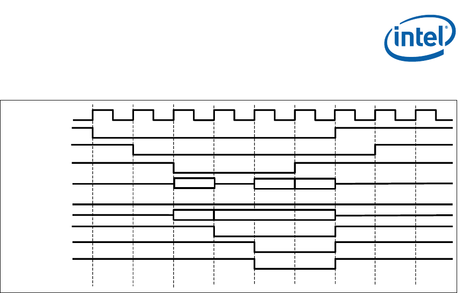
6.6.11 Initiated Burst Memory Write Transaction
The following transaction is a two word bursting PCI Memory Write Cycle initiated from
the IXP42X product line and IXC1100 control plane processors. This diagram is to
understand the inner workings of PCI transfers and may not reflect actual operation of
the PCI Controller implemented on the IXP42X product line and IXC1100 control plane
processors. The transaction is initiated to initial address location hexadecimal
0x00000014.
The value of binary 00 in PCI_AD (1:0) indicates that this is an linear increment
transfer type. The second data word transferred will be from address hexadecimal
0x00000018.
A hexadecimal value of 0x7 — written on the PCI_C/BE_N bus during the address
phase — signifies that this is a PCI Bus Memory Write Cycle. All byte-enables are active
for the transaction.
A maximum burst length of eight 32-bit words is supported for initiated Memory Cycle
transactions from the IXP42X product line and IXC1100 control plane processors.
Figure 43. Initiated PCI Burst Memory Read Cycle
PCI_CLK
PCI_FRAME_N
PCI_AD (31:0)
PCI_IDSEL
PCI_C/BE_N
PCI_IRDY_N
PCI_TRDY_N
PCI_DEVSEL_N
0x00000014
DATA 0
0x6 0x0
INT_REQ_N
INT_GNT_N
DATA 1


