Intel
®
IXP42X Product Line of Network Processors and IXC1100 Control Plane Processor
September 2006 DM
Order Number: 252480-006US 97
Intel XScale
®
Processor—Intel
®
IXP42X product line and IXC1100 control plane processors
When DBR1 is programmed as a data address mask, it is used in conjunction with the
address in DBR0. The bits set in DBR1 are ignored by the processor when comparing
the address of a memory access with the address in DBR0. Using DBR1 as a data
address mask allows a range of addresses to generate a data breakpoint. When DBR1
is selected as a data address mask, it is unaffected by the E1 field of DBCON. The mask
is used only when DBR0 is enabled.
When DBR1 is programmed as a second data address breakpoint, it functions
independently of DBR0. In this case, the DBCON.E1 controls DBR1.
A data breakpoint is triggered if the memory access matches the access type and the
address of any byte within the memory access matches the address in DBRx. For
example, LDR triggers a breakpoint if DBCON.E0 is 0b10 or 0b11, and the address of
any of the 4 bytes accessed by the load matches the address in DBR0.
The processor does not trigger data breakpoints for the PLD instruction or any CP15,
register 7, 8, 9, or 10 functions. Any other type of memory access can trigger a data
breakpoint. For data breakpoint purposes the SWP and SWPB instructions are treated
as stores - they will not cause a data breakpoint if the breakpoint is set up to break on
loads only and an address match occurs.
On unaligned memory accesses, breakpoint address comparison is done on a word-
aligned address (aligned down to word boundary).
When a memory access triggers a data breakpoint, the breakpoint is reported after the
access is issued. The memory access will not be aborted by the processor. The actual
timing of when the access completes with respect to the start of the debug handler
depends on the memory configuration.
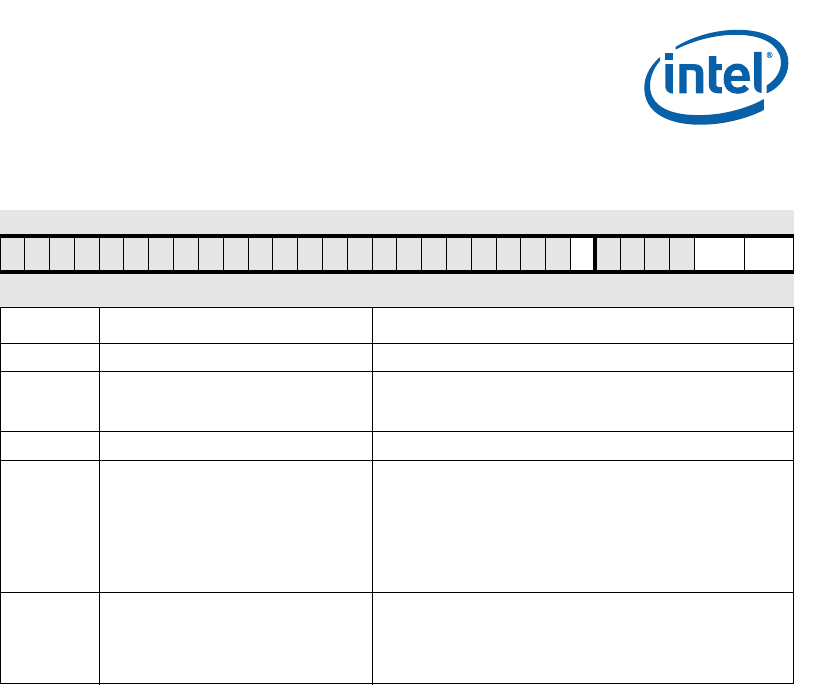
Table 37. Data Breakpoint Controls Register (DBCON)
31 30 29 28 27 26 25 24 23 22 21 20 19 18 17 16 15 14 13 12 11 10 9 8 7 6 5 4 3 2 1 0
M E1 E0
reset value: 0x00000000
Bits Access Description
31:9 Read-as-Zero / Write-ignored Reserved
8Read / Write
DBR1 Mode (M) -
0: DBR1 = Data Address Breakpoint
1: DBR1 = Data Address Mask
7:4 Read-as-Zero / Write-ignored Reserved
3:2 Read / Write
DBR1 Enable (E1) -
When DBR1 = Data Address Breakpoint
0b00: DBR1 disabled
0b01: DBR1 enabled, Store only
0b10: DBR1 enabled, Any data access, load or store
0b11: DBR1 enabled, Load only
When DBR1 = Data Address Mask this field has no effect
1:0 Read / Write
DBR0 Enable (E0) -
0b00: DBR0 disabled
0b01: DBR0 enabled, Store only
0b10: DBR0 enabled, Any data access, load or store
0b11: DBR0 enabled, Load only


