Intel
®
IXP42X Product Line of Network Processors and IXC1100 Control Plane Processor
September 2006 DM
Order Number: 252480-006US 359
Universal Asynchronous Receiver Transceiver (UART)—Intel
®
IXP42X product line and IXC1100
control plane processors
10.5.1.3 Divisor Latch Low Register
10.5.1.4 Divisor Latch High Register
Register THR
Bits Name Description
31:8 (Reserved)
7:0 THR
In Non-FIFO mode, This register holds the next data byte to be transmitted.
When the Transmit Shift Register becomes empty, the contents of the Transmit
Holding Register are loaded into the shift register and the transmit data request
(TDRQ) bit in the Line Status Register is set to 1.
In FIFO mode, writing to THR puts data to the top of the Transmit FIFO. The
data at the bottom of the Transmit FIFO is loaded to the shift register when the
shift register becomes empty.
The DLAB bit in the Line Control Register must be set to logic 0 to access this
register.
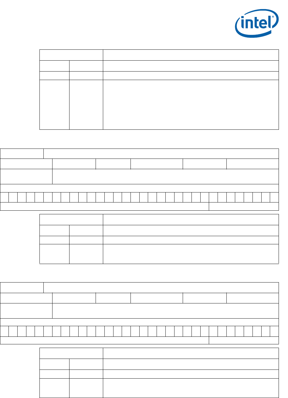
Register Name: DLL
Hex Offset Address: 0xC800 1000 Reset Hex Value: 0x00000002
Register
Description:
Divisor Latch Low Register
Access: Read/Write.
31 87 0
(Reserved) DLL
Register
DLL
Bits Name Description
31:8 (Reserved)
7:0 DLL
Lower byte of compare-value used by the baud-rate generator.
The DLAB bit in the Line Control Register must be set to logic 1 to access this
register.
Register Name: DLH
Hex Offset Address: 0xC800 1004 Reset Hex Value: 0x00000000
Register
Description:
Divisor Latch High Register
Access: Read/Write.
31 87 0
(Reserved) DLH
Register
DLH
Bits Name Description
31:8 (Reserved)
7:0 DLH
Upper byte of compare-value used by the baud rate generator.
The DLAB bit in the Line Control Register must be set to logic 1 to access this
register.


