Intel
®
IXP42X product line and IXC1100 control plane processors—Expansion Bus Controller
Intel
®
IXP42X Product Line of Network Processors and IXC1100 Control Plane Processor
DM September 2006
302 Order Number: 252480-006US
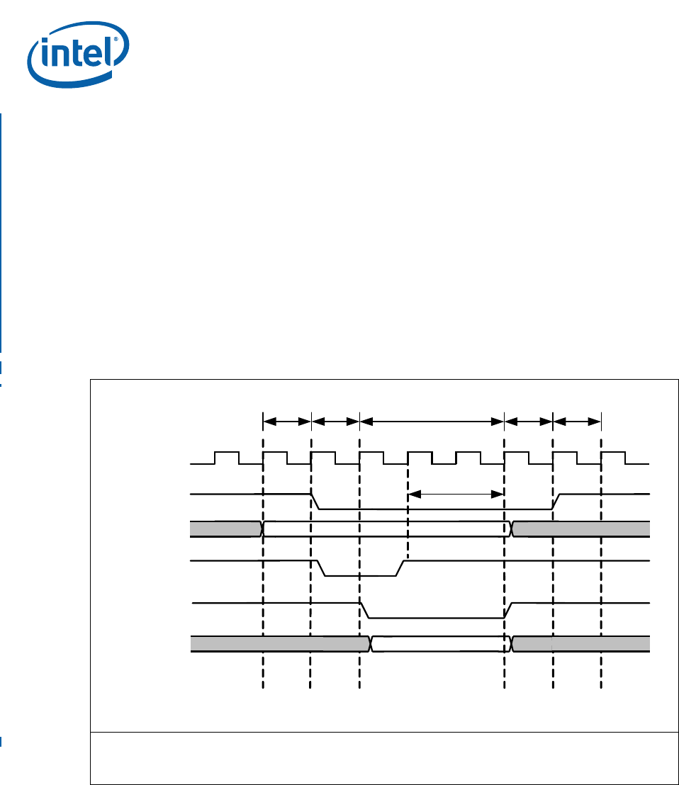
The T4 (Hold Timing) period is the time interval in which Chip Select will be held after
READ is deasserted. T4 prevents bus contention while Chip Select is asserted, in case
the peripheral driving the bus continues to send data out after READ has been
deasserted. During T4 no other transaction can start, since the current transaction will
not finish until Chip Select is deasserted by the processor.
T5 is the recovery time required before the next transaction can start.
The EX_IOWAIT_N signal only affects the interface during T2 when it is asserted and
during T3 when it is deasserted. If Chip Selects 4 through 7 are configured in HPI mode
of operation, each chip select will have a corresponding HRDY signal called EX_RDY.
The polarity of the ready signal is programmable. Chip Select 4 corresponds to EX_RDY
signal 0 and Chip Select 7 corresponds to EX_RDY signal 3.
In the case of extended phase timing, EX_IOWAIT_N is used in the same way as the
normal phase, however, the T1, T2, T4 and T5 periods take place over 4 cycles. T3 is
still programmable but each value is a multiple of 4 cycles. See Figure 62 for details.
Figure 61. I/O Wait Normal Phase Timing
Note: Notice that the access is an Intel-style simplex read access. The data strobe phase is set to a value to last
three clock cycles. The data is returned from the peripheral device prior to the three clocks and the
peripheral device de-asserts EX_IOWAIT_N. The data strobe phase terminates after two clocks even though
the strobe phase was configured to pulse for three clocks.
EX_CLK
EX_CS_N[0]
EX_ADDR[23:0]
EX_RD_N
EX_DATA[15:0]
Valid Data
Valid Address
1 Cycle 1 Cycle 3 Cycles 1 Cycle
T1=0 h T2=0 h T3=2h or 1h or 0h T4=0 h T5=0 h
EX_IOWAIT_N
B5242-01
1 Cycle
2 Cycles


