Intel
®
IXP42X Product Line of Network Processors and IXC1100 Control Plane Processor
September 2006 DM
Order Number: 252480-006US 481
Universal Serial Bus (USB) v1.1 Device Controller—Intel
®
IXP42X product line and IXC1100
control plane processors
18.5.1 UDC Control Register (UDCCR)
The UDC control register (UDCCR) contains seven control bits: one to enable the UDC,
one to show activity, and five to show status and associated control functions.
18.5.1.1 UDC Enable
The UDC Enable (UDE) bit enables the UDC. When UDE is set to a 1, the UDC is enabled
for USB serial transmission or reception. When UDE is set to a 0, the UDC is disabled
and the UDC+ and UDC- pins are tristated. This means that the UDC ignores all activity
on the USB bus.
If UDE is set to a 0 the entire UDC design is reset. If the reset occurs while the UDC is
actively transmitting or receiving data, it stops immediately and the remaining bits in
the transmit or receive serial shifter are reset.
All entries in the transmit and receive FIFO are also reset.
18.5.1.2 UDC Active
The read-only UDC Active (UDA) bit can be read to determine if the UDC is currently
active or in a USB reset. This bit is only valid when the UDC is enabled. A 0 indicates
that the UDC is currently receiving a USB reset from the USB Host. A 1 indicates that
the UDC is currently involved in a transaction.
18.5.1.3 UDC Resume (RSM)
When the UDC is in a suspend state, this bit can be written to force the UDC into a non-
idle state (K state) for 3 ms to perform a remote wake-up operation. If the host PC
does not start a wake-up sequence in 3 ms, the UDC returns to the suspend mode.
This bit is a trigger bit for the UDC and is automatically cleared.
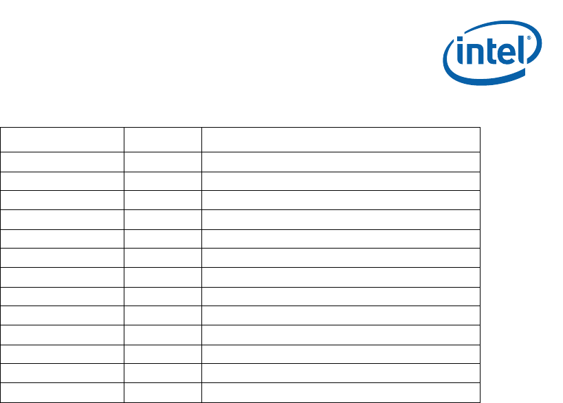
0 x C800 B200 UDDR3 UDC Endpoint 3 Data Register
0 x C800 B400 UDDR4 UDC Endpoint 4 Data Register
0 x C800 B0A0 UDDR5 UDC Endpoint 5 Data Register
0 x C800 B600 UDDR6 UDC Endpoint 6 Data Register
0 x C800 B680 UDDR7 UDC Endpoint 7 Data Register
0 x C800 B700 UDDR8 UDC Endpoint 8 Data Register
0 x C800 B900 UDDR9 UDC Endpoint 9 Data Register
0 x C800 B0C0 UDDR10 UDC Endpoint 10 Data Register
0 x C800 BB00 UDDR11 UDC Endpoint 11 Data Register
0 x C800 BB80 UDDR12 UDC Endpoint 12 Data Register
0 x C800 BC00 UDDR13 UDC Endpoint 13 Data Register
0 x C800 BE00 UDDR14 UDC Endpoint 14 Data Register
0 x C800 B0E0 UDDR15 UDC Endpoint 15 Data Register
Table 172. USB-Device Register Descriptions (Sheet 2 of 2)
Address Name Description


