Intel
®
IXP42X product line and IXC1100 control plane processors—SDRAM Controller
Intel
®
IXP42X Product Line of Network Processors and IXC1100 Control Plane Processor
DM September 2006
288 Order Number: 252480-006US
7.4.2 Refresh Register
The refresh register (SDR_REFRESH) is a read/write register and contains control bits
for refresh of the SDRAM banks. It holds the number of cycles before the Intel XScale
processor issues a mandatory refresh command. The SDRAM refresh interval field
applies to all types of SDRAM (asynchronous and synchronous).
7.4.3 Instruction Register
The instruction register is a read/write register that holds commands that are used to
determine the operation mode of the SDRAM controller and the mode register of the
SRDAM devices.
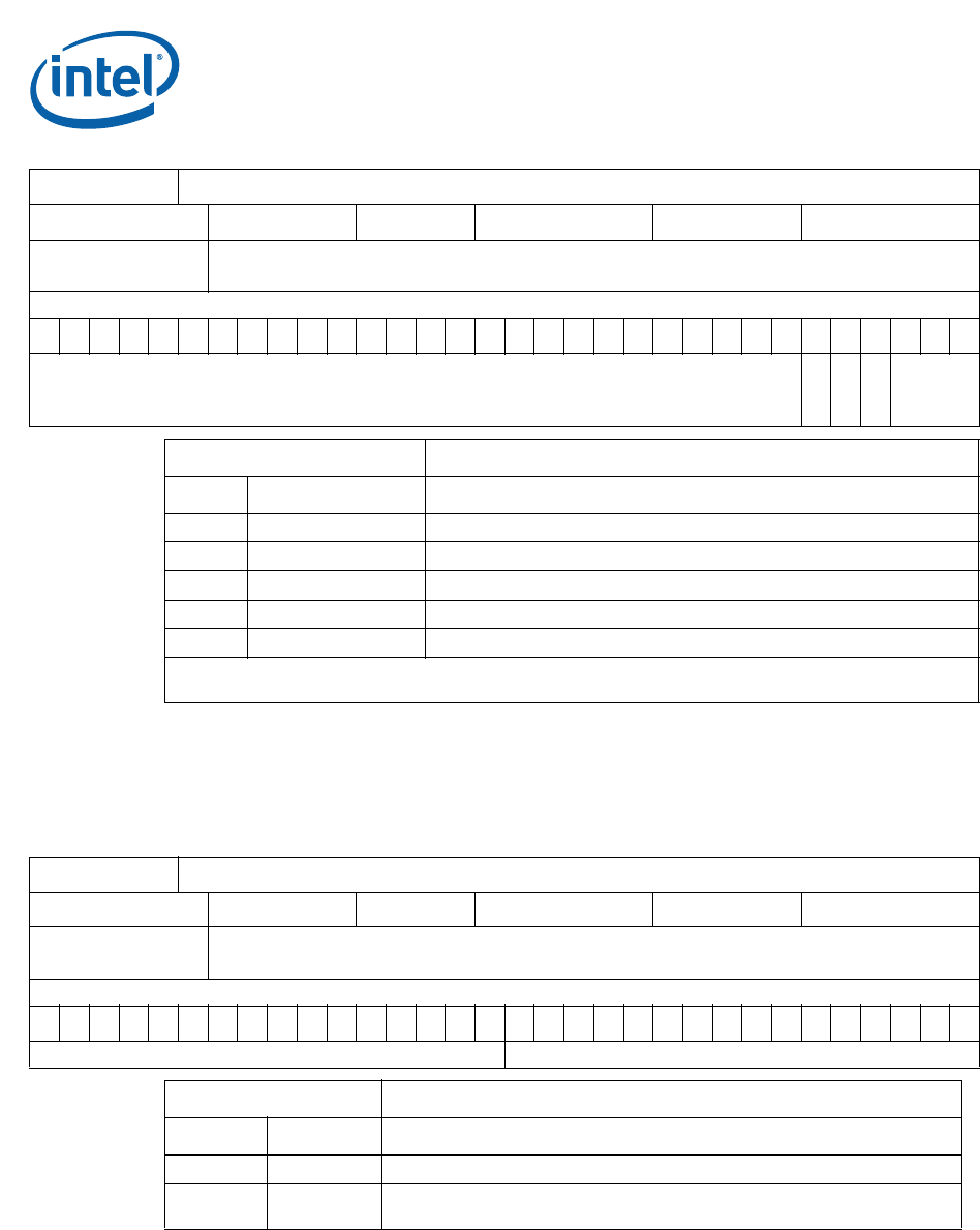
Register Name: SDR_CONFIG
Hex Offset Address: 0xCC000000 Reset Hex Value: 0x00000010
Register
Description:
Configuration of the memory/memory controller.
Access: Read/Write
31 5432 0
(Reserved)
64M en
RAS Lat
CAS Lat
Mem
config
Register
SDR_CONFIG
Bits Name Description
31:21 (Reserved) Reserved
5 Enable 64Mbit 1 = 64Mbit, 0 = 128/256/512 Mbit chips
4 RAS Latency 1 = Three-cycle latency. This is hard-coded.
3 CAS Latency 1 = Three-cycle latency. Default is two-cycle latency.
2:0 Memory Config Denotes memory size and type.
Note: It is possible to have different values sent to the SDRAM status mode register from what is written to
this register (cas/ras latencies). This may result in an undefined operation of the controller.
Register Name: SDR_REFRESH
Hex Offset Address: 0xCC000004 Reset Hex Value: 0x00000384
Register
Description:
Refresh register that holds Number of cycles before a mandatory refresh command is issued.
Access: Read/Write
31 16 15 0
(Reserved) Refresh Time
Register
SDR_REFRESH
Bits Name Description
31:16 (Reserved)
15:0 Refresh time
Number of cycles before a mandatory refresh command is issued. Defaults to
900 cycles.


