


©2008 Advanced Micro Devices, Inc.
SMBus Module and ACPI Block (Device 20, Function 0)
AMD SB600 Register Reference Manual Proprietary Page 101
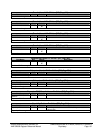
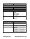
Base Address 2- R - 32 bits - [PCI_Reg: 18h]
Field Name Bits Default Description
Base Address 2 register
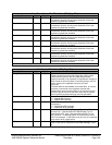
Base Address 3- R - 32 bits - [PCI_Reg: 1Ch]
Field Name Bits Default Description
Base Address 3 31:0 0000_000
0h
Not used and is hardcoded to 0.
Base Address 3 register
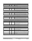
Base Address 4- R - 32 bits - [PCI_Reg: 20h]
Field Name Bits Default Description
Base Address 4 31:0 0000_000
0h
Not used and is hardcoded to 0.
Base Address 4 register
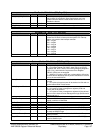
Base Address 5- R - 32 bits - [PCI_Reg: 24h]
Field Name Bits Default Description
Base Address 5 31:0 0000_000
0h
Not used and is hardcoded to 0.
Base Address 5 register
Cardbus CIS Pointer- R - 32 bits - [PCI_Reg: 28h]
Field Name Bits Default Description
Cardbus CIS Pointer 31:0 0000_000
0h
Not used and is hardcoded to 0.
Cardbus CIS Pointer register
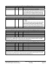
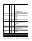
Subsystem Vendor ID- W - 16 bits - [PCI_Reg: 2Ch]
Field Name Bits Default Description
Subsystem Vendor ID 15:0 0000h Write once.
Subsystem Vendor ID register
Subsystem ID- W - 16 bits - [PCI_Reg: 2Eh]
Field Name Bits Default Description
Subsystem ID 15:0 0000h Write once.
Subsystem ID register
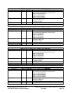
Expansion ROM Base Address - R - 8 bits - [PCI_Reg: 30h]
Field Name Bits Default Description
Expansion ROM Base
Address
7:0 00h Not used and is hardcoded to 0.
Expansion ROM Base Address register
Capability Pointer - R - 8 bits - [PCI_Reg: 34h]
Field Name Bits Default Description
Capability Pointer 7:0 B0/00h For K8 system default value is B0h; for P4 system default
value is 00h.
Capability Pointer register