©2008 Advanced Micro Devices, Inc.
AC ’97 Controller Functional Descriptions
AMD SB600 Register Reference Manual Proprietary Page 201
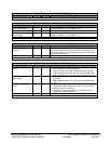
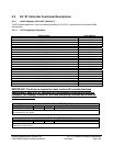
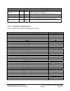
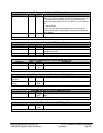
Base Address Reg 1- RW - 32 bits – [PCI_Reg: 14h]
Field Name Bits Default Description
Reserved 7:4 0h Always 0; meaning that the IO mapped registers occupy 256
bytes.
BAR1 31:8 0000_00h Base address register 1. Defines the base address for the
IO mapped register space of audio. This is to allow dual IO
and memory mapped addressing. In other words, if IO
mapping is enabled through this register, the IO indexed
registers are basically dual port as the memory mapped
registers. This register can only be programmed if index
50h, bit [1] is set. The purpose of this dual address
mapping is for diagnostics; not for OS usage
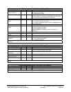
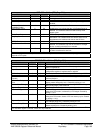
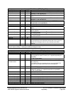
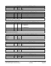
Subsystem ID & Subsystem Vendor ID – W/R – 32 bits – [PCI_Reg: 2Ch]
Field Name Bits Default Description
Subsystem Vendor ID 15:0 0000h Subsystem Vendor ID.
Subsystem ID 31:16 0000h Subsystem ID.
This 4-byte register is a write-once & read-only afterward register. The BIOS writes to this register once (all 4 bytes
at once) & software reads its value when needed.
Capabilities Pointer – R – 8 bits – [PCI_Reg: 34h]
Field Name Bits Default Description
Capabilities Pointer 7:0 40h Read only. Indicates that the device has New Capabilities
register set starting at address 40h.
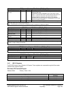
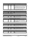
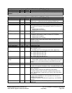
Interrupt Line – RW – 8 bits – [PCI_Reg: 3Ch]
Field Name Bits Default Description
Interrupt Line 7:0 00h Identifies which input of the system interrupt controller the
function’s PCI interrupt request pin (as specified in its
Interrupt Pin register) is routed to. The south bridge itself
does not use this value, rather it is used by device drivers
and operating systems.
Interrupt Pin – R – 8 bits – [PCI_Reg: 3Dh]
Field Name Bits Default Description
Interrupt Pin 7:0 02h Hard-wired to 2 to indicate that this function (audio
controller) uses interrupt pin INTB# on PCI bus..
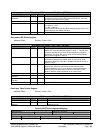
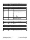
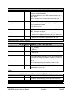
Min_Gnt – R – 8 bits – [PCI_Reg: 3Eh]
Field Name Bits Default Description
Min_Gnt 7:0 02h Hardwired to 2 to indicate the bus master would like to retain
PCI bus ownership for 500ns during a cycle.
Max_Lat – R – 8 bits – [PCI_Reg: 3Fh]
Field Name Bits Default Description
Max_Lat 7:0 00h Hard-wired to 0 to indicate the bus master has no stringent
requirement as to how often the device needs access to the
PCI bus.


