


©2008 Advanced Micro Devices, Inc.
Nomenclature and Conventions
AMD SB600 Register Reference Manual Proprietary Page 8
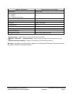
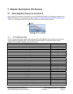
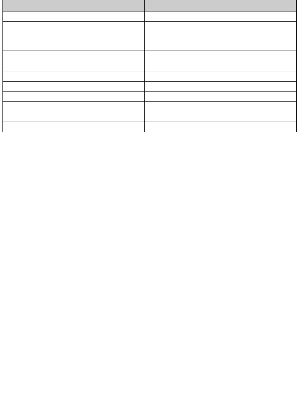
Register Information Value/Content in the Example
Register name Latency Timer
Read / Write capability
R = Readable
W = Writable
RW = Readable and Writable
RW
Register size 8 bits
Register address(es)* Offset: 0Dh
Field name Latency Timer (R/W)
Field position/size 7:0
Field default value 00h
Field description “This bit … 8 clocks.”
Field mirror information
Brief register description Latency Timer. Reset Value: 00h
* Note: There maybe more than one address; the convention used is as follows:
[aperName:offset] - single mapping, to one aperture/decode and one offset
[aperName1, aperName2, …, aperNameN:offset] - multiple mappings to different apertures/decodes but same
offset
[aperName:startOffset-endOffset] - mapped to an offset range in the same aperture/decode
Warning: Do not attempt to modify values of registers or bit fields marked "Reserved." Doing so may cause
the system to behave in unexpected manners.