


©2008 Advanced Micro Devices, Inc.
Real Time Clock (RTC)
AMD SB600 Register Reference Manual Proprietary Page 289
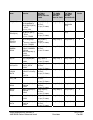
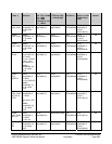
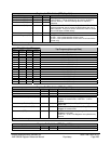
4.4 Real Time Clock (RTC)
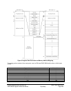
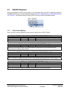
Note: Some RTC functions are controlled by, and associated with, certain PCI configuration registers in the
SMBus/ACPI device. For more information refer to section 2.3: SMBus Module and ACPI Block (Device 20,
Function 0). The diagram below lists these RTC functions and the associated registers.
RTC
RTC Ram Protection
External RTC Enable
RTC I/O Addr Enable
64h
6Ah 78h
PCI_Reg:
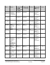
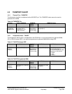
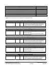
For software compatibility, the RTC registers and RAM are accessed through two banks addressing – Bank
0 and Bank 1, which are shown in the diagram below. Bank 0 is selected if DV0 = 0(DV0 is the 5
th
bit of
Register A) while Bank 1 is chosen if DV0 = 1. Even if two banks are defined, the first 64 bytes (00H – 3FH)
of each bank share the same physical space. The SB600 has alternate RAM ports at h72/h73 as the
address/data ports. These two ports do not use the bank0/bank1 scheme. Memory can be accessed
directly using the 8-bit address port. Use of the two IO ports h72/h73 to access the RTC RAM is
highly recommended.
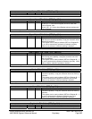
Note: Some RTC RAM space can be protected from read/write if corresponding bits are set to 1 in
RTCProtect register (PCI_Reg 6Ah).