


©2008 Advanced Micro Devices, Inc.
Host PCI Bridge Registers (Device 20, Function 4)
AMD SB600 Register Reference Manual Proprietary Page 270
IO Limit Upper 16 bits- RW - 16 bits - [PCI_Reg: 32h]
Field Name Bits Default Description
IO limit upper 16 bits
Capabilities Pointer- R - 8 bits - [PCI_Reg: 34h]
Field Name Bits Default Description
Capabilities Pointer 7:0 00h Enhanced Capability Pointer. Read Only.
Value = 54h when Offset 40h [3] MSI Guide Bit set to ‘1’
Capability Pointer register
Interrupt Line- R - 8 bits - [PCI_Reg: 3Ch]
Field Name Bits Default Description
Interrupt Line 7:0 00h Interrupt pin routing information, used as communication
window between BIOS and the device driver.
Interrupt Line register
Interrupt Pin- R - 8 bits - [PCI_Reg: 3Dh]
Field Name Bits Default Description
Interrupt Pin 7:0 00h Interrupt pin usage information. ‘0’ indicates PCIB not
supporting interrupt routing.
Interrupt Pin register
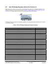
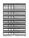
Bridge Control- RW - 16 bits - [PCI_Reg: 3Eh]
Field Name Bits Default Description
Parity Error Enable 0 0b Parity Error Response, ‘0’ disables PCIB to assert
P_SERR# and S_PERR# or report Detected Parity Error to
the secondary status register, ‘1’ enables PCIB.
Serr# Enable 1 0b SERR# forward enable, when ‘0’ PCIB doesn’t drive
P_SERR# when it detects S_SERR#.
ISA_Enable 2 0b ISA enable, when ‘0’ no ISA address mode, when ‘1’ ISA
address mode is supported.
VGA_Enable 3 0b VGA enable, ‘0’ disabled, ‘1’ enabled.
VGA 16-bit
decode
4 0b This bit only has meaning if either bit 3 (VGA Enable) of this
register, or bit 5 (VGA Palette Snoop Enable) of the
Command Register, is also set to 1, thereby enabling VGA
I/O decoding and forwarding by the bridge.
The status after reset is 0.
This read/write bit enables system configuration software to
select between 10- and 16-bit I/O address decoding for all
VGA I/O register accesses that are forwarded from primary
to secondary.
0 - Execute 10-bit address decodes on VGA I/O accesses.
1 - Execute 16-bit address decodes on VGA I/O
accesses
Master Abort Report 5 0b Master abort mode, ‘0’ does not report master aborts (return
FFFF,FFFFh on reads and discard data on write), ‘1’ reports
master aborts by signaling target abort or by asserting
SERR# if enabled.
Secondary Reset 6 0b Secondary bus reset, ‘0’ disabled, ‘1’ trigger reset.. This bit
can be masked using ACPI PCI config register x6c bit 5
Secondary Fast Back-
to-Back Enable
7 0b Secondary bus fast back-to-back enable. PCIB is not
capable of issuing fast back-to-back transactions on the
secondary bus. Read Only
Primary Discard Timer 8 0b Primary Discard Timer configuration, ‘0’ configures the timer
to 15-bit, ‘1’ configures the timer to 10-bit.