


©2008 Advanced Micro Devices, Inc.
AC ’97 Controller Functional Descriptions
AMD SB600 Register Reference Manual Proprietary Page 207
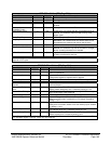
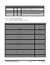
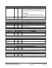
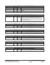
Slot Request- R - 32 bits - [MEM_Reg: 14h]
Field Name Bits Default Description
SLOTREQ 9:0 000h The read only bits [0:9] of this field respectively come from
slot1[11:2] of AC link’s SDATA_IN0/1/2 OR’ed together (even if slot
1 may not be valid as indicated by slot 0[14]). These bits [0:9]
respectively decide whether slot 3~12 of SDATA_OUT is allowed or
not.
0 – Slot is allowed
1 – Slot is allowed
Even if a bit in this field being 0 indicates a slot is allowed, the
controller further looks at reg0x34[9:0] to finally decide whether the
slot is enabled.
Reserved 31:10 000000
h
SLOTREQ Register
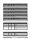
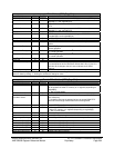
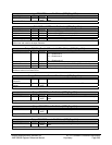
Counter- R - 32 bits - [MEM_Reg: 18h]
Field Name Bits Default Description
Slot Counter 3:0 0h The current slot number (0-12) which the AC97 controller handling.
Reserved 7:4 0h
Bit Clock Counter 12:8 00h For tag slot, the value changes from 0 to F. For other slots the value
changes from 0 to 20.
Reserved 31:13 00000h
Counter Register
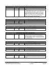
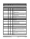
Input FIFO Threshold- RW - 32 bits - [MEM_Reg: 1Ch]
Field Name Bits Default Description
Input Threshold 4:0 00h Threshold value for the Input Channel's FIFOs. (FIFO size 16x20)
Reserved 31:5 000000
0h
Input FIFO Threshold Register: Input DMA's FIFOs threshold value.
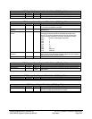
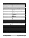
Input DMA Link List Pointer- RW - 32 bits - [MEM_Reg: 20h]
Field Name Bits Default Description
in DMA Link List
Pointer En
0 0b Input DMA Link List Pointer enable
in DMA Link List
Pointer
31:1 0000_0
000h
Pointer to the start of the Link List - to the first DT.
Input DMA Link List Pointer Register:
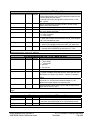
Input DMA DT Start- R - 32 bits - [MEM_Reg: 24h]
Field Name Bits Default Description
in DMA DT start 31:0 0000_0
000h
Pointer to the start of data associated with current DT for the input
DMA
Input DMA Discrete Table (DT) Start Pointer Register:
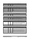
Input DMA DT Next- R - 32 bits - [MEM_Reg: 28h]
Field Name Bits Default Description
in DMA DT next 31:0 0000_0
000h
Pointer to the next DT for the input DMA
Input DMA DT Next Pointer Register: