


©2008 Advanced Micro Devices, Inc.
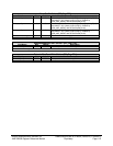
SMBus Module and ACPI Block (Device 20, Function 0)
AMD SB600 Register Reference Manual Proprietary Page 127
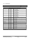
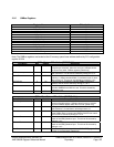
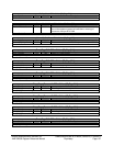
Register Name Offset Address
Dma2_Ch6Cnt CAh
Dma2_Ch7Addr CCh
Dma2_Ch7Cnt CEh
Dma_Status D0h
Dma_WriteRequest D2h
Dma_WriteMask D4h
Dma_WriteMode D6h
Dma_Clear D8h
Dma_Clear DAh
Dma_ClrMask DCh
Dma_ClrMask DEh
NCP_Error F0h
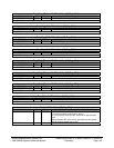
DMA1_Extend 40Bh
IntrEdgeControl 4D0h
DMA2_Extend 4D6h
Pci_Intr_Index C00h
Pci_Intr_Data C01h
Pci_Error C14h
CMIndex C50h
CMData C51h
GpmPort C52h
Isa_Misc C6Fh
PM2_Index CD0h
PM2_Data CD1h
BIOSRAM_Index CD4h
BIOSRAM_Data CD5h
PM_Index CD6h
PM_Data CD7h
.
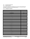
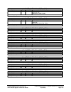
The PCI I/O registers are 32-bit registers decoded from the full 32-bit PCI address and C/BE[3:0]#.
Therefore, the bytes within a 32-bit address are selected with the valid byte enables. Registers and bits
within a register marked as reserved are not implemented. Writes have no effect on reserved registers. All
PCI I/O registers can be accessed via 8, 16, or 32-bit cycles (i.e., each byte is individually selected by the
byte enables).
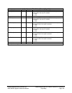
Dma_Ch 0- RW – 16 bits - [IO_Reg: 00h]
Field Name Bits Default Description
Dma_Ch 0 15:0 0000h DMA1 Ch0 Base and Current Address
Dma_Ch 0 register
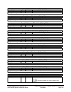
Dma_Ch 1- RW – 16 bits - [IO_Reg: 02h]
Field Name Bits Default Description
Dma_Ch 1 15:0 0000h DMA1 Ch1 Base and Current Address
Dma_Ch 1 register
Dma_Ch 2- RW – 16 bits - [IO_Reg: 04h]
Field Name Bits Default Description
Dma_Ch 2 15:0 0000h DMA2 Ch2 Base and Current Address
Dma_Ch 2 register
Dma_Ch 3- RW – 16 bits - [IO_Reg: 06h]
Field Name Bits Default Description
Dma_Ch 3 15:0 0000h DMA1 Ch3 Base and Current Address
Dma_Ch 3 register