


©2008 Advanced Micro Devices, Inc.
Host PCI Bridge Registers (Device 20, Function 4)
AMD SB600 Register Reference Manual Proprietary Page 271
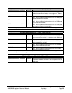
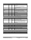
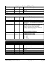
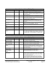
Bridge Control- RW - 16 bits - [PCI_Reg: 3Eh]
Field Name Bits Default Description
Secondary Discard
Timer
9 0b Secondary Discard Timer configuration, ‘0’ configures the
timer to 15-bit, ‘1’ configures the timer to 10-bit.
Discard Timer Status 10 0b Discard Timer Status, ‘0’ no discard timer error, ‘1’ discard
timer error.
Discard Timer Serr#
Enable
11 0b Discard Timer SERR# enable, ‘0’ disabled, ‘1’ enabled.
Reserved 15:12 0h Reserved
Bridge control register
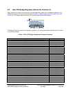
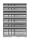
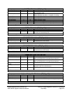
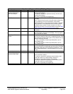
CPCTRL- RW - 8 bits - [PCI_Reg: 40h]
Field Name Bits Default Description
Reserved 0 0b Reserved
Mem Write Size Ctrl 1 0b Controls the Memory write size. When set the memory write
size will be cacheline aligned else it will be 32 byte aligned.
Lock Enable 2 1b Downstream locked transaction enable.
MSIC ap Enable 3 0b MSI Capability Enable Guide bit. ‘1’ enabled, ‘0’ disabled.
Setting this bit to ‘1’ will change the status of Offset 04h [20]
from ‘0’ to ‘1’
Prefetch Disable for
Upstream Mem Read
4 0b In A11~A13:
0: Prefetch is enabled for upstream normal memory read
(other than read line or read multiple). However, if
reg0x64[7]=0, then this prefetch is still disabled.
1: Prefetch is disabled for upstream normal memory read
(other than read line or read multiple).
In A21 and later versions: Reserved.
Also refer to reg0x64[7] and reg0x64[21].
Sub Decode Enable 5 0b This bit is used only when reg0x4B[7] = 1.
1: Subtractive decoding is enabled.
0: Subtractive decoding is disabled.
Bridge Lock State 7:6 00b Bridge secondary master lock states. Read Only
‘00’ – FREE
‘01’ – BUSY
‘10’ – REQ
‘11’ – LOCKED
Chip control register
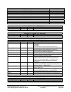
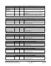
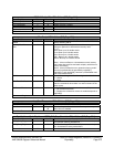
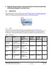
DCTRL- RW - 8 bits - [PCI_Reg: 41h]
Field Name Bits Default Description
Reserved 0 0b Reserved
Timer Test Mode 2:1 00b Timer Test Mode,
‘00’ – normal operation, all bits are exercised.
‘01’ – Byte 1 is exercised.
‘10’ – Byte 2 is exercised.
‘11’ – Byte 0 is exercised.
Force Parity Error 3 0b Force receiving/generating parity error, ‘0’ receiving, ‘1’
generating.
Force Data Parity Error 4 0b Force data parity error, ‘0’ disabled, ‘1’ enabled.
Force Addr Parity Error 5 0b Force address parity error, ‘0’ disabled, ‘1’ enabled.
Force Sec Parity Error 6 0b Force secondary Parity Error Mode, ‘0’ disabled, ‘1’ enabled.
Force Prim Parity Error 7 0b Force primary Parity Error Mode, ‘0’ disabled, ‘1’ enabled.
Diagnostic control register