


©2008 Advanced Micro Devices, Inc.
SMBus Module and ACPI Block (Device 20, Function 0)
AMD SB600 Register Reference Manual Proprietary Page 164
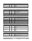
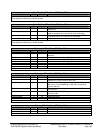
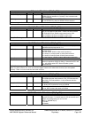
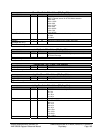
C4Control – RW – 8 bits – [PM_Reg:72h]
Field Name Bits Default Description
DPRSLPVR_delay 6:0 000_0000b This defines the delay between CPU_STP# de-assertion and
DPRSLPVR de-assertion in C4 state, in 2us increment with
2us uncertainty.
C4ChkVgate 7 0b 1: check VGATE=1 before DPRSLPVR de-assertion
0: use DPRSLPVR_delay for DPRSLPVR de-assertion
C4Control register for the P4 system.
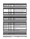
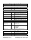
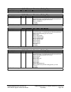
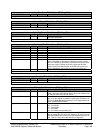
PopUpEndTime – RW – 8 bits – [PM_Reg:73h]
Field Name Bits Default Description
PopUpEndTime 7:0 80h This register applies to both P4 and K8 system. During C3/4
pop-up, SB monitors DMA traffic. If there has been no traffic
for PopUpEndTime, SB will bring system back to C3/4.
For P4 system, the time is counted by A-link clock.
For K8 system, the time is counted by OSC clock.
PopUpEndTime register
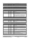
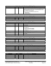
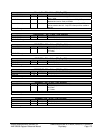
PwrFailShadow – RW – 8 bits – [PM_Reg:74h]
Field Name Bits Default Description
PwrFailShadow 3:0 0h Writing to these four bits will set the value onto bits [7:4].
Software should always set bit 2 = 1
PwrFailOption 5:4 00b These two bits will determine how system should resume after
a power failure.
00: Use default: Wait for wake event to power up
01: Always on: always power on after power resumes
10: Always off: always power off after power resumes
11: Use previous: resume to same setting when power fails.
PowerState 6 0b Power state indicator: 1 = on; 0 = off
ForcePwrOn 7 0b If set and RTC AIE =1, will force power on after power
resumes regardless of Bit[5:4] setting; if cleared and RTC AIE
= 1, will wakeup when RTC alarm fires after a power
failure/resume.
PwrFailShadow register
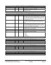
Note: For ASIC revisions A11, A12, and A13 this register needs to be written twice for bits [7:4] to be updated
correctly. There is no such restriction with other revisions.
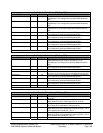
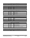
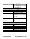
Tpreset1b – RW – 6 bits – [PM_Reg:75h]
Field Name Bits Default Description
Tpreset1b 5:0 05h Timing parameter used for S* -> S0 state transition.
This determines the delay between CPU_STP# de-assertion
and SUS_STAT# de-assertion, in 8us increment with 8us
uncertainty.
DelayRomRstEn 6 1b 1: 30ms ahead of deassertion of PciRst#
0: ROM_RST functions the same as PciRst#
DelayLanRstEn 7 1b 1: 20ms ahead of deassertion of PciRst#
0: Lan_RST functions the same as PciRst#
S0S3ToS5Enable0 – RW – 8 bits – [PM_Reg:76h]
Field Name Bits Default Description
S0S3ToS5Enable0 7:0 FFh This register determines which wakeup signals can be passed
onto the S5 region. For S4/S5 wake up, this bit must be set in
before the corresponding pin can be used
Bit [7:0]: GEVENT#[7:0]
1: Enable
0: Disable