©2008 Advanced Micro Devices, Inc.
Host PCI Bridge Registers (Device 20, Function 4)
AMD SB600 Register Reference Manual Proprietary Page 273
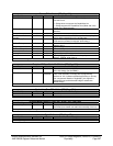
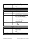
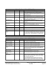
PCICLK Enable Bits- RW - 8 bits - [PCI_Reg: 4Ah]
Field Name Bits Default Description
PCICLK4Enable 0 1b 33MHz PCICLK4 enable.
PCICLK5Enable 1 1b 33MHz PCICLK 5 enable.
PCICLK6Enable 2 1b 33MHz PCICLK 6 enable.
PCICLK7Enable 3 1b 33MHz PCICLK 7 enable.
Reserved 7:4 3h Reserved
PCICLK Enable bits
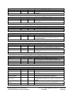
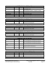
Misc Control RW - 8 bits - [PCI_Reg: 4Bh]
Field Name Bits Default Description
GNT Bus Idle check
enable
0 0b When enabled, the PCI arbiter checks for the Bus Idle
before asserting GNT#.
Memory Read Burst
Size
4:1 0h Specifies up to how many double words burst to support
during an upstream or downstream memory read.
[4:1] =
1xxx: Burst up to 16 double words
01xx: Burst up to 8 double words
001x: Burst up to 4 double words
0001: Burst up to 2 double words
Others: Burst up to 8 double words
Note 1: It has no effect on a downstream normal memory
read (other than read line and read multiple), which has no
burst in this design.
Note 2: It has no effective on an upstream memory read if
the read is prefetchable as specified by reg0x64[7],
reg0x64[21], and reg0x40[4], because a prefetchable read
can have unlimited burst.
IOMode 5 0b Control bit to change the IO addressing mode to 32/16 bit.
0 – 16 bits;
1 – 32 bit.
MemReadCmdMatch 6 0b Control bit to enable the match of memory read/memory
read line commands when there is a read command in the
delay queue.
SubDecodeEnable 7 0b Control bit for the subtractive decode status (09h).
0 – No subtractive decode;
1 – Whether the subtractive decode is enabled depends on
reg0x40[5].
Misc control Register
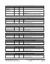
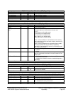
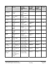
AutoClockRun control RW - 32 bits - [PCI_Reg: 4Ch]
Field Name Bits Default Description
Autoclkrun Enable 0 0b Enables the auto clkrun functionality
Autoclkrun count 31:1 0000_000
0h
Number of cycles after which the secondary clock stops
when clkrun is enabled
Auto ClockRun control register
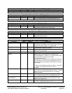
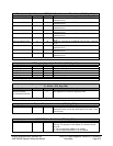
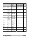
Dual Address Cycle Enable and PCIB_CLK_Stop Override - RW - 16 bits - [PCI_Reg: 50h]
Field Name Bits Default Description
PCIB_Dual_EN_up 0 0b Enables decoding of Dual Address Cycle on secondary side
for upstream memory transactions
PCIB_Dual_EN_dn 1 0b Enables decoding of Dual Address Cycle on secondary side
for downstream memory transactions
Reserved 5:2 0h


