


©2008 Advanced Micro Devices, Inc.
OCHI USB 1.1 and EHCI USB 2.0 Controllers
AMD SB600 Register Reference Manual Proprietary Page 47
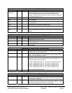
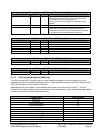
Status – R - 16 bits - [PCI_Reg : 06h]
Field Name Bits Default Description
Master Data
Parity Error
8 0b This bit is set only when three conditions are met: 1) the bus agent
asserted PERR# itself (on a read) or observed PERR# asserted (on a
write); 2) the agent setting the bit acted as the bus master for the
operation in which the error occurred; and 3) the Parity Error Response
bit (Command register) is set.
DEVSEL timing 10:9 01b Hard-wired to 01b – medium timing
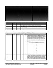
Signaled Target
Abort
11 0b This bit is set by a target device whenever it terminates a transaction
with Target-Abort.
Received Target
Abort
12 0b This bit is set by a master device whenever its transaction is terminated
with Target-Abort.
Received Master
Abort
13 0b This bit is set by a master device whenever its transaction (except for
Special Cycle) is terminated with Master-Abort.
Signaled System
Error
14 0b This bit is set whenever the device asserts SERR#.
Detected Parity
Error
15 0b This bit is set by the device whenever it detects a parity error, even if
parity error handling is disabled (as controlled by bit 6 in the Command
register).
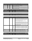
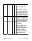
Revision ID / Class Code – R - 32 bits - [PCI_Reg : 08h]
Field Name Bits Default Description
Revision ID 7:0 00h Revision ID.
PI 15:8 10h Programming Interface. A constant value of ‘10h’ indentifies the device
being an OpenHCI Host Controller.
SC 23:16 03h Sub Class. A constant value of ‘03h’ indentifies the device being of
Universal Serial Bus.
BC 31:24 0Ch Base Class. A constant value of ‘0Ch’ identifies the device being a Serial
Bus Controller.
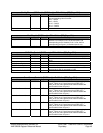
Miscellaneous – RW/R - 32 bits - [PCI_Reg : 0Ch]
Field Name Bits Default Description
Cache Line Size 7:0 00h This read/write field specifies the system cacheline size in units of
DWORDs and must be initialized to 00h.
Latency Timer 15:8 00h [9:8] hard-wired to 00b, resulting in a timer granularity of at least four
clocks. This field specifies, in units of PCI bus clocks, the value of the
Latency Timer for this PCI bus master.
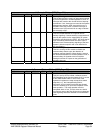
Header Type 23:16 80h/00h This field identifies the layout of the second part of the predefined header
(beginning at byte 10h in Configuration Space) and also whether or not
the device contains multiple functions.
Function 0: Bit[23] hard-wired to 1 Æ the device has multiple functions.
Function 1: Bit[23] hard-wired to 0 Æ the device is single function.
Function 2: Bit[23] hard-wired to 0 Æ the device is single function.
Function 3: Bit[23] hard-wired to 0 Æ the device is single function.
Function 4: Bit[23] hard-wired to 0 Æ the device is single function.
Bits [22:16] are hard-wired to 00h.
BIST 31:24 00h Hard-wired to 00h, indicating no build-in BIST support.
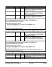
Bar_OHCI – RW - 32 bits - [PCI_Reg : 10h]
Field Name Bits Default Description
IND 0 0b Indicator. A constant value of ‘0’ indicates that the operational registers
of the device are mapped into memory space of the main memory of the
PC host system. Read Only.
TP 2:1 0h Type. A constant value of ‘00b’ indicates that the base register is 32-bit
wide and can be placed anywhere in the 32-bit memory space; i.e., lower
4 GB of the main memory of the PC host. Read Only.