


©2008 Advanced Micro Devices, Inc.
HD Audio Controllers Registers
AMD SB600 Register Reference Manual Proprietary Page 232
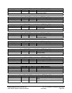
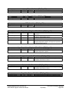
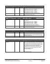
MSI Message Lower Address – RW - 32 bits – [PCI_Reg: 64h]
Field Name Bits Default Description
MSI Message Lower
Address
31:2 00000000
h
Lower Address used for MSI Message.
Reserved 01:0 0h Reserved
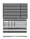
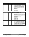
MSI Message Upper Address – RW - 32 bits – [PCI_Reg: 68h]
Field Name Bits Default Description
MSI Message Upper
Address
31:0 00000000
h
Upper Address used for MSI Message.
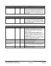
MSI Message Data – RW - 16 bits – [PCI_Reg: 6Ch]
Field Name Bits Default Description
MSI Message Data 15:0 0000h Data used for MSI Message.
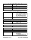
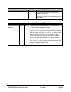
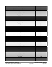
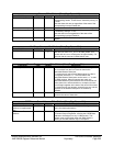
2.6.2 HD Audio Controller Memory Mapped Registers
The base memory location for these memory mapped registers is specified in the PCI Configuration Upper
and Lower Base Address Registers. The individual registers are then accessible at Base + offset as
indicated in the following table. These registers are accessed in byte, word, or dword quantities.
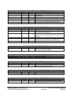
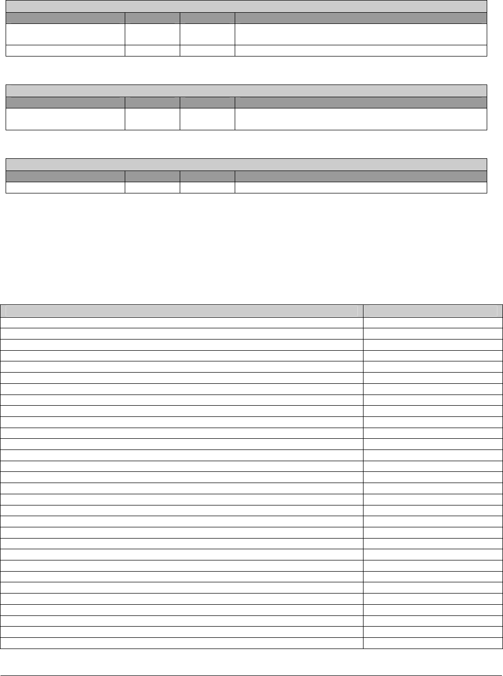
Register Name Address Offset
Global Capabilities 00h
Minor Version 02h
Major Version 03h
Output Payload Capability 04h
Input Payload Capability 06h
Global Control 08h
Wake Enable 0Ch
State Change Status 0Eh
Global Status 10h
Output Stream Payload Capability 18h
Input Stream Payload Capability 1Ah
Interrupt Control 20h
Interrupt Status 24h
Wall Clock Counter 30h
Stream Synchronization 38h
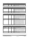
CORB Lower Base Address 40h
CORB Upper Base Address 44h
CORB Write Pointer 48h
CORB Read Pointer 4Ah
CORB Control 4Ch
CORB Status 4Dh
CORB SIze 4Eh
RIRB Lower Base Address 50h
RIRB Upper Address 54h
RIRB Write Pointer 58h
RIRB Response Interrupt Control 5Ah
RIRB Control 5Ch
RIRB Status 5Dh
RIRB Size 5Eh
Immediate Command Output Interface 60h