


©2008 Advanced Micro Devices, Inc.
SMBus Module and ACPI Block (Device 20, Function 0)
AMD SB600 Register Reference Manual Proprietary Page 102
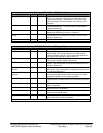
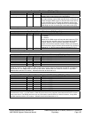
Interrupt Line - R - 8 bits - [PCI_Reg: 3Ch]
Field Name Bits Default Description
Interrupt Line 7:0 00h This module does not generate interrupt. This register is
hardcoded to 0.
Interrupt Line register
Interrupt Pin – R - 8 bits - [PCI_Reg: 3Dh]
Field Name Bits Default Description
Interrupt Pin 7:0 00h This register specifies which interrupt pin the device issues.
This module does not generate interrupt but contains the
actual interrupt controller. This register is hardcoded to 0.
Interrupt Pin register
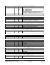
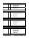
Min_Gnt - R - 8 bits - [PCI_Reg: 3Eh]
Field Name Bits Default Description
Min_Gnt 7:0 00h This register specifies the desired settings for Latency Timer
values. Value of 0 indicates that the device has no major
requirements for the setting. This value is hardcoded to 0.
Min_Gnt register
Max_Lat - R - 8 bits - [PCI_Reg: 3Fh]
Field Name Bits Default Description
Max_Lat 7:0 00h This register specifies the desired settings for Latency Timer
values. Value of 0 indicates that the device has no major
requirements for the setting. This value is hardcoded to 0.
Max_Lat register
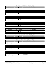
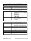
PCI Control- RW - 8 bits - [PCI_Reg: 40h]
Field Name Bits Default Description
Reserved 1:0 00b
KB2RstEnable 2 0b When set, KeyBoard reset (KBRST#) pin will generate a
system wide reset (ARST#) for P4 system; for K8 system,
additional control by PMIO 66h Bit 5 determines whether INIT#
or ARST# is generated
Reserved 7:3 0h
PCI Control register
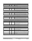
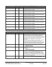
MiscFunction- RW - 8 bits - [PCI_Reg: 41h]
Field Name Bits Default Description
Reserved 0 0b
ExtraROM AddrEnable2 1 0b This bit only has meaning if xbus ROM is used. If this bit is
set, addresses between FFF80000h to FFFDFFFFh will be
directed to the ROM interface
Reserved 2 0b
WatchDogDecodeEn 3 0b Enables watchdog decode
ExtraROM AddrEnable1 4 0b This bit is meaningful if ROM interface is strapped to the xbus
ROM (sits on PCI bus). If this bit is set, addresses between
0E0000h to 0EFFFFh will be directed to the ROM interface.
MiscfuncEnable 5 0b When set, this module will decode cycles to IO C50, C51, C52:
GPM controls.
Reserved 7:6 00b
MiscFunction register