


©2008 Advanced Micro Devices, Inc.
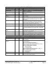
SATA Registers (Device 18, Function 0)
AMD SB600 Register Reference Manual Proprietary Page 15
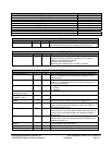
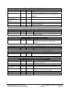
Status - RW - 16 bits - [PCI_Reg:06h]
Field Name Bits Default Description
Reserved 2:0 Reserved.
Interrupt Status 3 0b Interrupt status bit. Complies with the PCI 2.3 specification.
Capabilities List 4 1b Read Only. Hardwired to 1 to indicate that the Capabilities
Pointer is located at 34h.
66MHz Support 5 1b 66MHz capable. This feature is supported in the SATA
controller.
Reserved 6
Reserved.
Fast Back-to-Back
Capable
7 0b Read Only. Hard-wired to ‘0’ to indicate that it is fast back to
back incapable.
Data Parity Error 8 0b Data Parity reported. Set to 1 if the SATA controller detects
PERR- asserted while acting as the PCI master (whether
PERR- was driven by the SATA controller or not.). Write ‘1’ to
clear this bit.
DEVSEL- Timing 10:9 01b Read only.
These bits indicate DEVSEL- timing when performing a
positive decode. Since DEVSEL- is asserted to meet the
medium timing, these bits are encoded as 01b.
Signaled Target Abort 11 0b Signaled Target Abort. This bit is set to 1, when the SATA
controller signals Target Abort. Write ‘1’ to clear this bit.
Received Target Abort 12 0b Received Target Abort. This bit is set to 1 when the SATA
controller that generated the PCI cycle (SATA controller is the
PCI master) is aborted by a PCI target. Write ‘1’ to clear this
bit.
Received Master Abort
Status
13 0b Received Master Abort Status. Set to 1 when the SATA
controller, acting as a PCI master, aborts a PCI bus memory
cycle. Write ‘1’ to clear this bit..
SERR- Status 14 0b SERR- status. This bit is set to 1 when the SATA controller
detects a PCI address parity error. Write ‘1’to clear this bit.
Detected Parity Error 15 0b Detected Parity Error. This bit is set to 1 when the SATA
controller detects a parity error. Write ‘1’ to clear this bit.
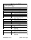
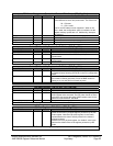
Revision ID/Class Code- R - 32 bits - [PCI_Reg:08h]
Field Name Bits Default Description
Revision ID 7:0 00h These bits are hardwired to 00h to indicate the revision level of
the chip design.
Operating Mode
Selection
15:8 8Fh RW
Programmable I/F.
Bit [15] = Master IDE Device. Always 1.
Bits [14:12] = Reserved. Always read as 0’s.
Bit [11] = Programmable indicator for Secondary. Always 1 to
indicate that both modes are supported.
Bit [10] = Operating Mode for Secondary.
1 = Native PCI-mode.
0 = Compatibility Mode
Bit [9] = Programmable indicator for Primary. Always 1 to
indicate that both modes are supported.
Bit [8] = Operating Mode for Primary.
1 = Native PCI-mode.
0 = Compatibility
Sub-Class Code 23:16 01h Sub-Class Code. 01h to indicate an IDE Controller. See Note.
Class Code 31:24 01h Class Code. These 8 bits are read only and wired to 01h to
indicate a Mass-Storage Controller.