


©2008 Advanced Micro Devices, Inc.
LPC ISA Bridge (Device 20, Function 3)
AMD SB600 Register Reference Manual Proprietary Page 257
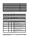
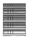
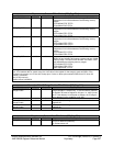
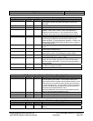
Firmware Hub Select – RW* - 32 bits - [PCI_Reg: 70h]
Field Name Bits Default Description
FWH_D8_IDSEL 15:12 4h IDSEL for two 512 KB FWH memory ranges. The IDSEL
programmed in this field addresses the following memory
ranges:
FFD8 0000h-FFDF FFFFh
FF98 0000h-FF9F FFFFh
FWH_E0_IDSEL 19:16 3h IDSEL for two 512 KB FWH memory ranges. The IDSEL
programmed in this field addresses the following memory
ranges:
FFE0 0000h-FFE7 FFFFh
FFA0 0000h-FFA7 FFFFh
FWH_E8_IDSEL 23:20 2h IDSEL for two 512 KB FWH memory ranges. The IDSEL
programmed in this field addresses the following memory
ranges:
FFE8 0000h-FFEF FFFFh
FFA8 0000h-FFAF FFFFh
FWH_F0_IDSEL 27:24 1h IDSEL for two 512 KB FWH memory ranges. The IDSEL
programmed in this field addresses the following memory
ranges:
FFF0 0000h-FFF7 FFFFh
FFB0 0000h-FFB7 FFFFh
FWH_F8_IDSEL 31:28 0h Read only.
IDSEL for two 512 KB FWH memory ranges and one 128KB
memory range. This field is fixed at 0000. The IDSEL in this
field addresses the following memory ranges:
FFF8 0000h-FFFF FFFFh
FFB8 0000h-FFBF FFFFh
000E 0000h-000F FFFFh
This register is used to generate the 4-bit IDSEL phase when LPC does read/write to firmware hub memory on LPC
bus. If PCI address falls in certain range, the 4-bit value in the register for that range is used as IDSEL. Every
firmware hub memory on LPC bus has 4 strap pins. If value on those pins matches IDSEL from LPC host, the
memory is selected.
*bit [31:28] read only
Default Value: 01234567h
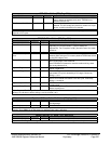
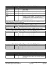
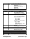
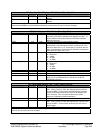
Alternative Wide IO Range Enable- RW - 32 bits - [PCI_Reg: 74h]
Field Name Bits Default Description
Alternative Wide Io
Range Enable
0 0b Wide IO range is usually 512 bytes. With this bit set, the
range changes to 16 bytes only. To use this feature, address
in reg0x64~65 must be aligned to 16 bytes, i.e., bit[3:0] must
be 0. If the address is not aligned to 16bytes, the IO range is
from address [15:0] to {address [15:4], 0xF}.
Reserved 1 0h
Alternative Wide Io 1
Range Enable
2 0h Similar to bit 0, but it applies to the IO address defined in
reg0x66~67.
Alternative Wide Io 2
Range Enable
3 0h Similar to bit 0, but it applies to the IO address defined in
reg0x90~91.
Reserved 7:4 00h
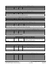
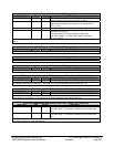
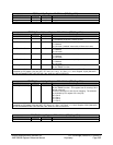
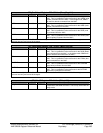
Miscellaneous Control Bits- RW - 8 bits - [PCI_Reg: 78h]
Field Name Bits Default Description
DMA_Enhance 0 1b 1—Turn on the enhancement feature for the DMA function.
This is for better bus efficiency
0—Enhancement off.