©2008 Advanced Micro Devices, Inc.
AC ’97 Controller Functional Descriptions
AMD SB600 Register Reference Manual Proprietary Page 215
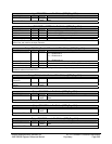
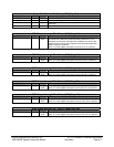
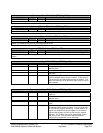
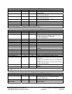
Cache Line Size - RW - 8 bits - [PCI_Reg: 0Ch]
Field Name Bits Default Description
Cache Line Size 7:0 00h Cache Lien Size.
Cache Line Size Register: This register specifies the system cache line size.
Latency Timer - RW - 8 bits - [PCI_Reg: 0Dh]
Field Name Bits Default Description
Latency Timer 7:0 00h Latency Timer.
Latency Timer Register: This register specifies the value of the Latency Timer in units of PCICLKs.
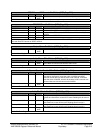
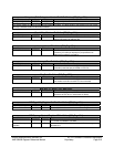
Header Type - R - 8 bits - [PCI_Reg: 0Eh]
Field Name Bits Default Description
Header Type 7:0 80h Header Type.
Header Type Register: This register identifies the type of the predefined header in the configuration space. Since
SB600 is a multifunction device, the most significant bit is set.
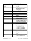
BIST- R - 8 bits - [PCI_Reg: 0Fh]
Field Name Bits Default Description
BIST 7:0 00h BIST.
Built-in Self Test Register: This register is used for control and status for Built-in Self Test. Ac97 has no BIST
modes.
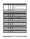
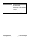
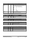
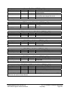
Base Address Reg 0- RW* - 32 bits – [PCI_Reg: 10h]
Field Name Bits Default Description
MemoryIndicator 0 0b Always 0; meaning it is always memory mapped
Type 2:1 00b Always 0; meaning it can be located anywhere in 32 bit
address space
Prefetchable 3 0b Always 0; meaning it is not prefetchable
Reserved 7:4 0h Always 0; meaning the memory mapped registers occupy
256 bytes
BAR0 31:8 0000_00h Base address register 0. Defines the base address for the
memory mapped register space of modem. If index 50h, bit
3 is set, bits [13:8] of this register become unwritable. The
effect will cause the OS to allocate a wider memory map for
this controller.
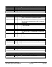
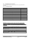
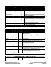
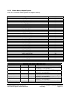
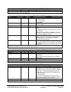
Base Address Reg 1- RW* - 32 bits – [PCI_Reg: 14h]
Field Name Bits Default Description
MemoryIndicator 0 0b This bit will return 1 if index 50h, bit [1] is set. 1 means IO
mapping.
Type 2:1 00b Always 0; meaning it can be located anywhere in 32 bit
address space
Prefetchable 3 0b Always 0; meaning it is not prefetchable
Reserved 7:4 0h Always 0; meaning the IO mapped registers occupy 256
bytes
BAR1 31:8 0000_00h Base address register 1. Defines the base address for the
IO mapped register space of modem. This is to allow dual
IO and memory mapped addressing. In other words, if IO
mapping is enabled through this register, the IO indexed
registers are basically dual port as the memory mapped
registers. This register can only be programmed if index
50h, bit [1] is set. The purpose of this dual address
mapping is for diagnostics; not for OS usage


