


©2008 Advanced Micro Devices, Inc.
AC ’97 Controller Functional Descriptions
AMD SB600 Register Reference Manual Proprietary Page 218
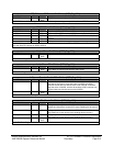
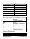
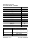
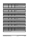
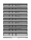
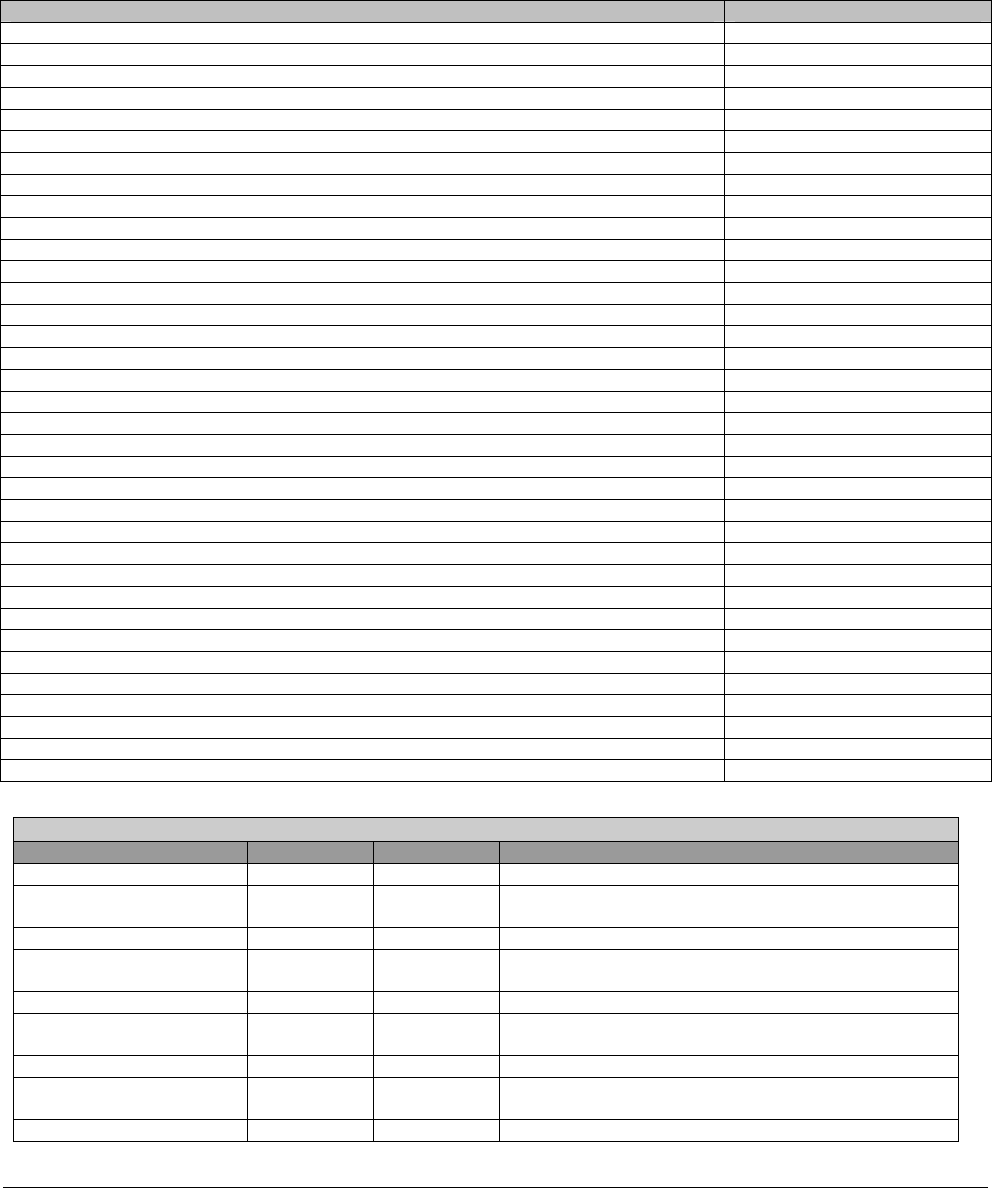
2.5.2.2 Modem Memory Mapped Registers
All the AC’97 Controller modem registers are mapped to memory.
Register Name Offset Address
Interrupt 00h
Interrupt Enable 04h
Modem Command 08h
Output Phy Status And Address 0Ch
Input Phy Address & Data 10h
SLOTREQ 14h
Counter 18h
Input Fifo Threshold 1Ch
Input DMA Link List Pointer 20h
Input DMA DT Start 24h
Input DMA DT Next 28h
Input DMA DT Current 2Ch
Input DT Size And FIFO Info 30h
Out Fifo's Threshold 34h
Output DMA1 Link List Pointer 38h
Output DMA2 Link List Pointer 3Ch
Output DMA3 Link List Pointer 40h
Output DMA1 DT Start 44h
Output DMA1 DT Next 48h
Output DMA1 DT Current 4Ch
Output DMA2 DT Start 50h
Output DMA2 DT Next 54h
Output DMA2 DT Current 58h
Output DMA3 DT Start 5Ch
Output DMA3 DT Next 60h
Output DMA3 DT Current 64h
Output DMA 1/2 Size 68h
Output DMA 3 DT Size 6Ch
Output Dma 1/2/3 Fifo Info 70h
Output GPIO Out Data 74h
Input GPIO Data 78h
Modem Mirror 7Ch
Audio Mirror 80h
Modem FIFO Flush 88h
Phy Semphore Register A8h
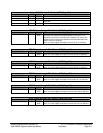
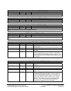
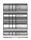
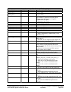
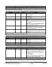
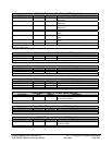
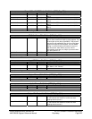
Interrupt - RW - 32 bits - [MEM_Reg: 00h]
Field Name Bits Default Description
in DMA Overflow 0 0b Input Channel overflow - out of FIFO space
in DMA Status 1 0b Input Channel status bit - set to "1" after finishing DT
(if reg0x04[1]=1 and reg0x08[5]=1)
out DMA1 Underflow 2 0b Output DMA1 underflow - no data in FIFO
out DMA1 Status 3 0b Output DMA1 status bit - set to "1" after finishing DT (if
reg0x04[1]=1 and reg0x08[5]=1)
out DMA2 Underflow 4 0b Output DMA2 underflow - no data in FIFO
out DMA2 Status 5 0b Output DMA2 status bit - set to "1" after finishing DT (if
reg0x04[1]=1 and reg0x08[5]=1)
out DMA3 Underflow 6 0b Output DMA3 underflow - no data in FIFO
out DMA3 Status 7 0b Output DMA3 status bit - set to "1" after finishing DT (if
reg0x04[1]=1 and reg0x08[5]=1)
Phy Data Incoming 8 0b Got OR’ed Phy register address and data from Codecs