


©2008 Advanced Micro Devices, Inc.
AC ’97 Controller Functional Descriptions
AMD SB600 Register Reference Manual Proprietary Page 214
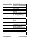
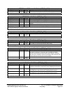
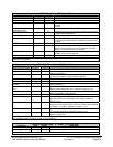
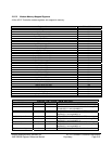
CMD- RW - 16 bits - [PCI_Reg: 04h]
Field Name Bits Default Description
IO Space 0 0b I/O Access Enable.
Memory Space 1 0b Memory Access Enable.
Bus Master 2 0b Master Enable
Special Cycles 3 0b Hardwired to 0 to indicate that Special Cycle recognition is
disabled.
Memory Write and
Invalidate Enable
4 0b Memory Write and Invalidate Enable.
VGA Palette Snoop 5 0b Hardwired to 0 to indicate that the controller does not need
to snoop VGA palette cycles.
Parity Error Response 6 0b PERR# (Response) Detection Enable bit
Stepping Control 7 0b Hardwired to 0 to indicate that the controller does not need
to insert a wait state between the address and data on the
AD lines.
SERR# Enable 8 0b SERR# enable
Fast Back-to-Back Enable 9 0b Hardwired to 0 to indicate that Fast Back-to-back is
disabled. The controller only acts as a master to a single
device, so this functionality is not needed.
INTB# Enable# 10 0b When it is 0, INTB# is allowed to send out. When it is 1,
INTB# is not allowed to send out.
Reserved 15:11 00h
Command Register: The PCI specification defines this register to control a PCI device’s ability to generate and
respond to PCI cycles.
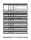
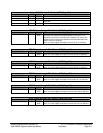
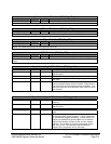
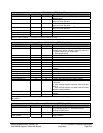
STATUS- RW - 16 bits - [PCI_Reg: 06h]
Field Name Bits Default Description
Reserved 2:0 0h
Interrupt B status 3 0b When there is interrupt B, this bit will be 1, regardless of the
value in reg0x04[10].
Capabilities List 4 1b Read only. Indicates that the new capabilities list pointer
configuration register is implemented in reg0x34.
66MHz-Capable 5 1b Read only. Indicates that device is capable of running at 66MHz.
Reserved 6 0b
Fast Back-to-Back
Capable
7 0b Read only. Indicates that device does not support fast back-to-
back transactions.
Master Data Parity
Error
8 Master Data Parity Error. This bit is set to 1 when the controller
detects master data parity error. Cleared by writing a 1 to it.
Device Select Timing 10:9 10b DEVSEL# timing – Read only bits indicating DEVSEL# timing
when performing a positive decode.
Signaled Target Abort 11 0b Read only. The device does not support target aborts.
Received Target Abort 12 0b Received Target Abort .This bit is set to 1 when the controller
generated PCI cycle is aborted by a PCI target. Cleared by
writing a 1 to it.
Received Master Abort 13 0b Received Master Abort Status. Set to 1 when the controller
acting as a PCI master, aborts a PCI bus memory cycle. Cleared
by writing a 1 to this bit. Cleared by writing a 1 to it.
Signaled System Error 14 0b SERR# status. This bit is set to 1, when the controller detects a
PCI address parity error. Cleared by writing a 1 to it.
Detected Parity Error 15 0b Detected Parity Error. This bit is set to 1 when the controller
detects a parity error.
Status Register: The PCI specification defines this register to record status information for PCI related events. This
is a read/write register. However, writes can only reset bits.
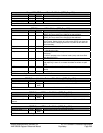
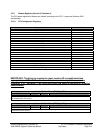
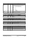
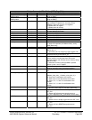
Revision ID/Class Code – R - 32 bits - [PCI_Reg: 08h]
Field Name Bits Default Description
Revision ID 7:0 00h
Class Code 31:8 070300h Class Code.
Revision ID Register: This read only register contains the device’s revision information and generic function.