


©2008 Advanced Micro Devices, Inc.
LPC ISA Bridge (Device 20, Function 3)
AMD SB600 Register Reference Manual Proprietary Page 255
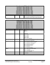
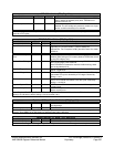
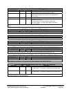
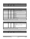
Rom Protect 0 - RW - 32 bits - [PCI_Reg: 50h]
Field Name Bits Default Description
Write Protect 0 0b When this bit is set, the memory range defined by this register is
write-protected. Writing to the range has no effect.
Read Protect 1 0b When this bit is set, the memory range defined by this register is
read-protected. Reading any location in the range returns
FFFF_FFFFh.
Rom Offset 10:2 000h Rom range offset
Rom Base 31:11 000000h Rom Base and Rom Offset together define the ROM range to be
protected. The range is:
From {Rom Base, 000_0000_0000b} to {Rom Base,
000_0000_0000b} + {0_0000_0000_0000b, Rom Offset,
11_1111_1111b}
This register is write/read, but it can only be written once after hardware reset. Subsequent writes to it have no
effect.
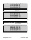
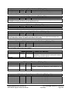
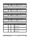
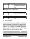
Rom Protect 1 - RW - 32 bits - [PCI_Reg: 54h]
Field Name Bits Default Description
This register has exactly the same definition as that of Rom Protect 0.
Rom Protect 2 - RW - 32 bits - [PCI_Reg: 58h]
Field Name Bits Default Description
This register has exactly the same definition as that of Rom Protect 0.
Rom Protect 3 - RW - 32 bits - [PCI_Reg: 5Ch]
Field Name Bits Default Description
This register has exactly the same definition as that of Rom Protect 0.
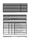
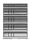
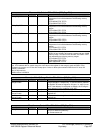
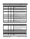
PCI Memory Start Address for LPC Target Cycles - RW - 16 bits - [PCI_Reg: 60h]
Field Name Bits Default Description
Memory Start Address 15:0 0000h 16-bit starting address of the LPC target (memory) range.
This register contains upper 16-bits of the starting address of the LPC memory target range. The lower 16-bits of
the starting address are considered 0’s. This range can be enabled/disabled using register 48h, bit 5.
PCI Memory End Address for LPC Target Cycles - RW - 16 bits - [PCI_Reg: 62h]
Field Name Bits Default Description
Memory End Address 15:0 0000h 16-bit END address of the LPC target (memory) range.
This register contains upper 16-bits of the ending address of the LPC memory target range. The lower 16-bits of the
end address are considered 1’s. This range can be enabled/disabled using register 48h, bit 5.
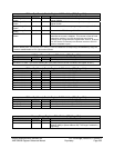
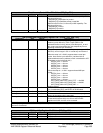
PCI IO base Address for Wide Generic Port - RW - 16 bits - [PCI_Reg: 64h]
Field Name Bits Default Description
IO Base Address 0 15:0 0000h 16-bit PCI IO base address for wide generic port range. 512
byte wide range. This function is enabled by PCI register 48h,
bit 2
IO Base Address 1 31:16 0000h 16-bit PCI IO base address for wide generic port range. 512
byte wide range. This function is enabled by PCI register 4Bh,
bit 0
This register contains two 16-bits of IO base address for LPC IO (wide generic port) target range. The limit address
is found by adding 512 to the base address.