


©2008 Advanced Micro Devices, Inc.
About this Manual
AMD SB600 Register Reference Manual Proprietary Page 7
1 Introduction
1.1 About this Manual
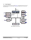
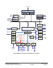
This manual is a register reference guide for the AMD SB600 Southbridge. It integrates the key I/O,
communications, and audio features required in a state-of-the-art PC into a single device. It is specifically
designed to operate with AMD’s RADEON IGP Xpress family of integrated graphics processor products in
both desktop and mobile PCs.
1.2 Nomenclature and Conventions
1.2.1 Recent Updates
Updates recent to each revision are highlighted in red.
1.2.2 Numeric Representations
• Hexadecimal numbers are prefixed with “0x” or suffixed with “h,” whenever there is a possibility
of confusion. Other numbers are decimal.
• Registers (or fields) of an identical function are sometimes indicated by a single expression in
which the part of the signal name that changes is enclosed in square brackets. For example,
registers HOST_DATA0 through to HOST_DATA7 is represented by the single expression
HOST_DATA[7:0].
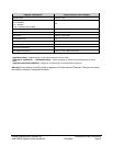
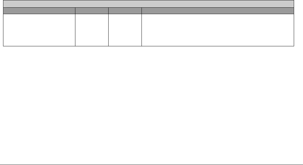
1.2.3 Register Description
All registers in this document are described with the format of the sample table below. All offsets are
in hexadecimal notation, while programmed bits are in either binomial or hexadecimal notation.
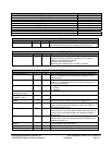
Table 1-1: Register Description Table Notation—Example
Latency Timer – RW – 8 bits – [Offset: 0Dh]
Field Name Bits Default Description
Latency Timer (R/W) 7:0 00h This bit field is used to specify the time in number of PCI
clocks, the SATA controller as a master is still allowed to
control the PCI bus after its GRANT_L is deasserted. The
lower three bits [0A:08] are hardwired to 0
h , resulting in a
time granularity of 8 clocks.
Latency Timer. Reset Value: 00h