


©2008 Advanced Micro Devices, Inc.
HD Audio Controllers Registers
AMD SB600 Register Reference Manual Proprietary Page 238
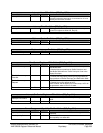
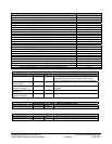
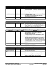
Interrupt Status – RW – 32 bits - [Mem_Reg: Base + 24h]
Field Name Bits Default Description
Stream Interrupt Status 7:0 00h A “1” indicates that an interrupt condition occurred on the
corresponding stream. These bits are cleared by writing 1’s
to them.
Note that these bits are set regardless of the state of the
corresponding Interrupt Enable bits.
Reserved 29:8 000000h Reserved
Controller Interrupt Status 30 0b A “1” indicates that an interrupt condition occurred. This bit
is cleared by writing a “1” to it.
Note that this bit is set regardless of the state of the
corresponding Interrupt Enable bit.
Global Interrupt Status 31 0b This bit is an “OR” of all the interrupt status bits in this
register.
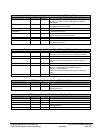
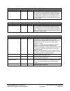
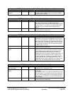
Wall Clock Counter – R – 32 bits - [Mem_Reg: Base + 30h]
Field Name Bits Default Description
Wall Clock Counter 31:0 00000000
h
32 bit counter that Is incremented at the link bitclock rate
and rolls over from FFFF_FFFFh to 0000_0000h. This
counter will roll over to 0 with period of approximately 179
seconds with the nominal 24 MHz bitclock rate.
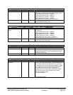
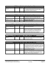
Stream Synchronization – RW – 32 bits – [Mem_Reg: Base + 38h]
Field Name Bits Default Description
Stream Synchronization 7:0 00h When these bits are set, they block data from being sent
on or received from the link. Each bit controls the
associated Stream Descriptor.
To synchronously start a set of DMA engines, the bits in
this register are set to a “1”. The RUN bits for the
associated Stream Descriptors can be set to a “1” to start
the DMA engines. When all streams are ready, the
associated Stream Synchronization bits can all be set to 0
at the same time, and transmission or reception from the
link will begin together at the start of the next full link frame.
To synchronously stop streams, these bits are set, and the
RUN bits in the Stream Descriptors are cleared by
software.
Reserved 31:8 000000h Reserved. Software must do a read-modify-write to
preserve the value of these bits.
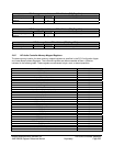
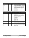
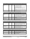
CORB Lower Base Address – RW – 32 bits – [Mem_Reg: Base + 40h]
Field Name Bits Default Description
CORB Lower Base
Address Unimplemented
Bits
6:0 00h Hardwired to 0. This forces 128-byte buffer alignment for
cache line fetch optimizations.
CORB Lower Base
Address
31:7 0000000h Upper 25 bits of the 32 bits Lower Base address of the
Command Output Ring Buffer, allowing the CORB Base
Address to be assigned on any 1 KB boundary. This
register must not be written when the DMA engine is
running or the DMA transfer may be corrupted.