


©2008 Advanced Micro Devices, Inc.
IDE Controller (Device 20, Function 1)
AMD SB600 Register Reference Manual Proprietary Page 192
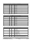
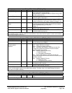
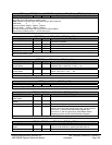
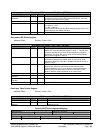
IDE Legacy DMA (Multi-words DMA) Timing Modes - RW - 32 bits - [PCI_Reg:44h]
Field Name Bits Default Description
IDE Legacy DMA (Multi-words DMA) Timing Modes Register: This register controls the IDE interface and selects
the timing of the IDE DMA bus-master cycles.
Note: Relation of setting value and actual timing of each mode are
DMA Mode 2 1 0
Command Width 2(90ns) 2(90ns) 7(240ns)
Recover Width 0(30ns) 1(60ns) 7(240ns)
The above timings are valid and A-Link clock is always 66MHz.
Actual timing is setting value + 1 A-Link clock cycle.
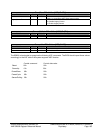
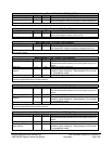
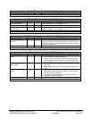
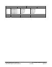
IDE PIO Control - RW - 16 bits - [PCI_Reg:48h]
Field Name Bits Default Description
Primary IDE Disable 0 0b Disable Primary IDE controller. When set Primary IDE
controller is disabled.
Reserved 3:1 000b Reserved. Always read as 0’s
Reserved 8:4 00h Obsolete bits
Reserved 11:9 000b Reserved. Always read as 0’s
Reserved 15:12 0h Obsolete bits
IDE PIO Control Register: This register controls the IDE interface and selects the control functions of the PCI bus
IDE PIO bus-master cycles.
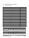
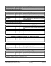
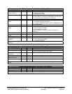
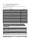
IDE PIO Mode - RW- 16 bits - [PCI_Reg:4Ah]
Field Name Bits Default Description
Primary Master PIO
Access Mode
2:0 0h PIO access mode for Primary IDE Master device. For
instance, PIO 0 = 000, PIO 1 = 001, … etc..
Reserved 3 0b Reserved. Always read as 0’s.
Primary Slave PIO
Access Mode
6:4 0h PIO access mode for Primary IDE Slave device. For instance,
PIO 0 = 000, PIO 1 = 001, … etc..
Reserved 15:7 000h Reserved. Always read as 0’s.
IDE PIO Mode Register: This register specifies PIO modes primary channel.
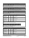
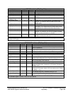
IDE Status - R- 8 bits - [PCI_Reg:4Ch]
Field Name Bits Default Description
Reserved 7:0 00h Reserved. These bits always read as0’s.
IDE Status Register: This register specifies the IDE Status of primary channel.
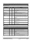
IDE Ultra DMAControl - RW- 8 bits - [PCI_Reg:54h]
Field Name Bits Default Description
Primary Master Ultra
DMA enable
0 0b Ultra DMA Enable Primary IDE Master device.
Primary Slave Ultra DMA
enable
1 0b Ultra DMA Enable Primary IDE Slave device.
Reserved 6:2 00000b Reserved. Always read as 0’s.
Ultra DMA Report Mode 7 0b Report Mode.
When host receives last data as extra word, reporting will be:
If this bit is 1, set IDE Ultra DMA Status register only.
If this bit is 0, clear the interrupt bit of BusMaster Status
Register and also set IDE Ultra DMA Status Register.
IDE Ultra DMA Control Register: This register specifies the IDE Control of primary channel.
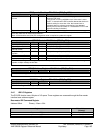
IDE Ultra DMA Status - RW- 8 bits - [PCI_Reg:55h]
Field Name Bits Default Description
Primary Extra Data
Status
0 0b Transaction is complete, but internal buffer has some data.
This bit will be cleared by resetting the DMA start bit.
Reserved 7:1 00h Reserved. Always read as 0’s.