


©2008 Advanced Micro Devices, Inc.
IDE Controller (Device 20, Function 1)
AMD SB600 Register Reference Manual Proprietary Page 195
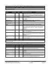
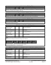
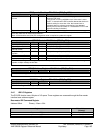
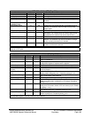
IDE Dynamic Clocking - RW- 20 bits - [PCI_Reg:6Ch]
Field Name Bits Default Description
IDE Power Down
Counter
19:0 FFFFFh The IDE power down counter can be programmed to shut
down the IDE clock.
The counter is running at 66Mhz clock. If the value is set to
0x3FF, it means that the IDE controller detects that the bus is
without activity for more than 15us, the internal clock is
powered down for advance power saving. Any detected
activity will turn the clock back on. The default is FFFFFh and
dynamic clocking is disabled.
Reserved 31:20 000h Reserved. Always wired as 0’s.
IDE Dynamic Clocking Register: This register specifies the time (in number of IDE clocks) to shut down the IDE
clock after there are no more IDE transactions.
Note: A 32-bit double-word (DW) PCI configuration write is required to update this register.
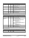
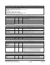
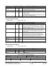
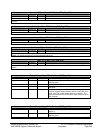
IDE MSI Control - RW- 32 bits - [PCI_Reg:70h]
Field Name Bits Default Description
Capability ID 7:0 05h Capability ID (hard_wired to 05h)
Capability Next Pointer 15:8 00h Next Pointer (hard_wired to 00h)
Message Signaled
Interrupt Enable
16 0b MSI Enable (MSI_En)
Multiple Message
Capable
19:17 0h Multiple Message Capable (MMC)
Multiple Message Enable 22:20 0h Multiple Message Enable (MME) (hard_wired to 0h)
MSI 64-bit Address 23 0b 64-bit address (hard_wired to 0b)
Reserved 31:24 00h Reserved. Always wired as 0’s.
IDE MSI Control Register: This register specifies MSI Capability ID, next pointer, MSI enable, multiple message
capable, multiple message enable bits.
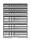
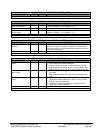
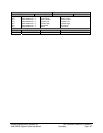
IDE MSI Address Register - RW- 32 bits - [PCI_Reg:74h]
Field Name Bits Default Description
IDE MSI Address 31:0 0000_0000h MSI Address
IDE MSI Address Register: This register specifies MSI address.
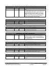
IDE MSI Data Register - RW- 16 bits - [PCI_Reg:78h]
Field Name Bits Default Description
IDE MSI Data 15:0 0000h MSI Data
IDE MSI Data Register: This register specifies MSI data.
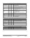
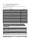
2.4.2 IDE I/O Registers
The PCI IDE function uses 16 bytes of I/O space. These registers are accessed through the Bus-master
interface base address register.
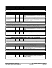
Bus-master IDE Command Register
Address Offset: Primary – Base + 00h
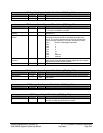
Register Name Offset Address
[Primary]
Bus-master IDE Command 00h/08h
Bus-master IDE Status 02h/0Ah
Bus-master IDE Command 04h/0Ch