


©2008 Advanced Micro Devices, Inc.
GEVENT/GPE/GPM/ExtEvent
AMD SB600 Register Reference Manual Proprietary Page 287
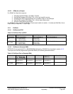
4.2.3.2 GPM pins as Output
For GPM[7:0], follow this sequence -
1. Set index register 0C50h to 13h (Misc. Control).
2. Set CM Data register 0C51h Bits [7:6] = 01b to set Input/Out control.
3. Set GPM port 0C52h appropriate bits to 0 to enable output on the GPM port.
4. Set CM Data register 0C51h Bits [7:6] = 10b for output data control.
5. Write the output data to port 0C52h.
For GPM[9:8], simply use PM I/O 95h Bits [1:0] as output enable (0: enable; 1: tri-state) and 94h Bits [1:0] as
output value (0: output low; 1: output high).
4.2.4 ExtEvent
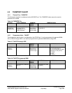
4.2.4.1 ExtEvent as GPIO
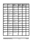
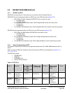
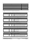
Table 4-4: ExtEvent Pins as GPIO
Pin Name Output Enable Output Register Input Status
EXTEVNT0#/
RI#
PM IO Reg91h[Bit 0]
0: Output enable
1: Input (Tri-state)
PM IO Reg90h[Bit 0]
0: Output low
1: Output high
PM IO Reg0Dh[Bit 0]
EXTEVNT1#/
LPC_SMI#
PM IO Reg91h[Bit 1]
0: Output enable
1: Input(Tri-state)
PM IO Reg90h[Bit 1]
0: Output low
1: Output high
PM IO Reg0Dh[Bit 1]
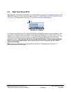
4.2.4.2 ExtEvent to Generate SMI#
EXTEVNT[1:0] can generate SCI or SMI#/SMI#/SMI# followed by SCI/IRQ13 as described in section 4.2.2.
These pins can also be programmed to generate SMI# by the following alternate method.
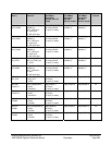
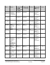
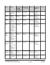
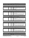
Table 4-5: ExtEvent Pins to Generate SMI#
Pin Name* Trigger
1 – Rising edge
0 – Falling edge
Enable SMI# SMI# Status Logical Value
Read only
Power Domain
EXTEVNT0#/
RI#
PM IO
Reg0Dh[Bit 2]
PM IO
Reg04h[Bit 0]
PM IO
Reg07h[Bit 0]
PM IO
Reg0Dh[Bit 0]
S5
EXTEVNT1#/
LPC_SMI#
PM IO
Reg0Dh[Bit 3]
PM IO
Reg04h[Bit 1]
PM IO
Reg07h[Bit 1]
PM IO
Reg0Dh[Bit 1]
S0