


©2008 Advanced Micro Devices, Inc.
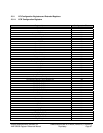
SMBus Module and ACPI Block (Device 20, Function 0)
AMD SB600 Register Reference Manual Proprietary Page 97
2.3.1 PCI Configuration Registers and Extended Registers
2.3.1.1 PCIE Configuration Registers
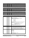
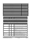
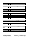
Register Name Configuration Offset
VendorID 00h
DeviceID 02h
Command 04h
STATUS 06h
Revision ID/Class Code 08h
Cache Line Size 0Ch
Latency Timer 0Dh
Header Type 0Eh
BIST 0Fh
Base Address 0 10h
Base Address 1 14h
Base Address 2 18h
Base Address 3 1Ch
Base Address 4 20h
Base Address 5 24h
Cardbus CIS Pointer 28h
Subsystem Vendor 2Ch
Subsystem ID 2Eh
Expansion ROM Base Address 30h
Capability Pointer 34h
Interrupt Line 3Ch
Interrupt Pin 3Dh
Min_Gnt 3Eh
Max_Lat 3Fh
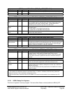
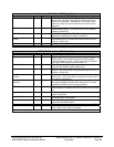
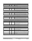
PCI Control 40h
MiscFunction 41h
DmaLimit 42h
DmaEnhanceEnable 43h
ISA Address Decode Control Register #1 48h
ISA Address Decode Control Register #2 49h
GPIO_52_to_49_Cntrl 50h
GPIO_56_to_53_Cntrl 52h
GPIO_60_to_57_Cntrl 54h
GPIO_64_to_61_Cntrl 56h
GPIO_73_to_70_Cntrl 5Ah
SmartPowerControl1 5Ch
SmartPowerControl2 5Dh
MiscEnable 62h
AzIntMap 63h
Features Enable 64h
SeriallrqControl 69h
RTCProtect 6Ah
USB Reset 6Bh
TestMode 6Ch
IoApic_Conf 74h
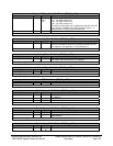
IoAddrEnable 78h
GPIO_69_68_66_65_Cntrl 7Eh
GPIO_3_to_0_Cntrl 80h
GPIO_32_31_14_13_Cntrl 82h
Smbus Base Address 90h
IDE_GPIO_Cntrl A0h