


©2008 Advanced Micro Devices, Inc.
IDE Controller (Device 20, Function 1)
AMD SB600 Register Reference Manual Proprietary Page 188
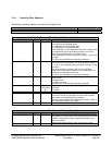
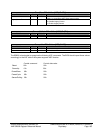
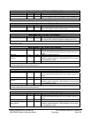
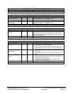
Status - RW - 16 bits - [PCI_Reg:06h]
Field Name Bits Default Description
DEVSEL- Timing 10:9 01b DEVSEL- timing – Read only bits indicating DEVSEL- timing
when performing a positive decode.
Since DEVSEL- is asserted to meet the medium timing, these
bits are encoded as 01b.
Signaled Target Abort 11 0b Signaled Target Abort – This bit is set to 1, when the IDE host
controller signals Target Abort.
Received Target Abort 12 0b Received Target Abort – This bit is set to 1 when the IDE host
controller-generated PCI cycle (IDE host controller is the PCI
master) is aborted by a PCI target. Cleared by writing a 1 to it.
Received Master Abort
Status
13 0b Received Master Abort Status. Set to 1 when the IDE host
controller acting as a PCI master, aborts a PCI bus memory
cycle. Cleared by writing a 1 to this bit.
Default - 0.
SERR- Status 14 0b SERR- status. This bit is set to 1 when the IDE host controller
detects a PCI address parity error.
Detected Parity Error 15 0b Detected Parity Error. This bit is set to 1 when the IDE host
controller detects a parity error.
Status Register: The PCI specification defines this register to record status information for PCI related events. This
is a read/write register. However, writes can only reset bits. A bit is reset when the register is written and the data in
the corresponding bit location is a 1.
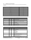
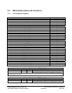
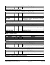
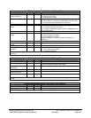
Revision ID/Class Code- RW - 32 bits - [PCI_Reg:08h]
Field Name Bits Default Description
Revision ID 7:0 00h These bits are hardwired to 00h to indicate the revision level of
the chip design (for the SB600).
IDE Host Controller
Operating Mode
Selection
15:8 8Ah Programmable I/F. These 8 bits are read/write.
Bit 7 – Master IDE Device. Always 1.
Bit 6-4 – Reserved. Always read as 0’s.
Bit 3 – Secondary IDE Enable bit. Setting this bit with PCI
configuration offset 0x49 bit 8 back to back will disable
secondary IDE host controller.
Bit 2 – Operating Mode for Secondary.
1 = Native PCI-mode.
0 = Compatibility Mode(Default).
Bit 1 – Primary IDE Enable bit. Setting this bit with PCI
configuration offset 0x49 bit 0 back to back will disable primary
IDE host controller.
Bit 0 – Operating Mode for Primary.
1 = Native PCI-mode.
0 = Compatibility mode (Default).
Sub-Class Code 23:16 01h Sub-Class Code. These 8 bits are read only and wired to 01h
to indicate an IDE Controller.
Class Code 31:24 01h Class Code. These 8 bits are read only and wired to 01h to
indicate a Mass-Storage Controller.
Revision ID/Class Code Register: This register contains the device’s revision information, generic function of a
device, and the specific register level programming interface. The Base class is 01h (Mass-Storage Controller),
Sub-class is 01h (IDE Controller).
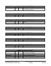
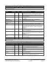
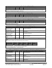
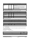
Cache Line Size - RW - 8 bits - [PCI_Reg:0Ch]
Field Name Bits Default Description
Cache Line Size Register 7:0 00h If the value is 10 that means the cache line size is 16 DW (64
byte).
Cache Line Size Register: This register specifies cache line size and the default value is 00.