


©2008 Advanced Micro Devices, Inc.
AC ’97 Controller Functional Descriptions
AMD SB600 Register Reference Manual Proprietary Page 206
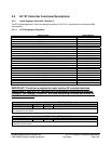
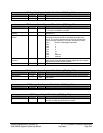
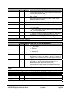
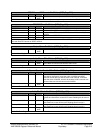
Audio Command- RW - 32 bits - [MEM_Reg: 08h]
Field Name Bits Default Description
Packed format disable 24 0b 1 - Disable packed format for sending data: data is sent to memory
including data from Slot1 and 2 (physical address and data are send
to memory along with other data).
0 - Data send to memory through DMA in packed format, no slot 1
and 2 - default
Burst enable. 25 0b Enable DMA operation in burst mode: Will send/request data only
based on threshold value & overflow condition. All other cases
(lowest priority) will be disabled.
Panic enable 26 0b Enable panic signal - to get more priority over internal bus.
Modem_slots_alloc_0 27 0b Mirror bit of modem memory mapped register0x08[27]. Refer to that
bit for more detailed information.
AC Link active 28 0b Read only.
0 - AC Link is not active;
1 - AC Link is active.
AC'97 software reset 29 0b 0 – De-assert ac97 software reset asynchronous to BIT_CLK;
1 – Assert ac97 software reset asynchronous to BIT_CLK. Registers
in BIT_CLK domain will be reset.
AC97 Sync 30 0b 0 – De-assert AC link’s SYNC asynchronous to BIT_CLK
1 – Assert AC link’s SYNC asynchronous to BIT_CLK. After being
asserted, the bit will automatically deassert itself in one clock.
AC97 Reset# 31 0b 0 – Assert AC link’s RESET# asynchronous to BIT_CLK;
1 – De-assert AC link’s RESET# asynchronous to BIT_CLK
Audio Command Register: Controls the operation of Audio Controller. Value of "1" in bit position enables
corresponding function. Value of "0" disables it.
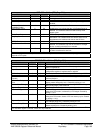
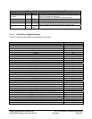
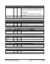
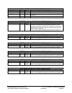
Phy Out Address and Data- RW - 32 bits - [MEM_Reg: 0Ch]
Field Name Bits Default Description
Codec ID 1:0 0b 0 – Master AC97
1 – 1
st
slave AC97
2 – 2
nd
slave AC97
3 – Reserved
Read/Write request 2 0b 1 – Read request.
0 – Write request
Reserved 7:3 0h
Phy out enable 8 0b 1 - Enable sending out of Physical address in next frame
0 - Physical out address have been sent out; open to get new value.
When the bit is 0, writing 1 to it makes it 1. Once it is 1, writing to it
is ignored. It will automatically return to 0 when physical address is
sent out.
Phy out address 15:9 00h Physical out address (will not be able to write new address until old
one is send out - until Physical out address enable is '1') (for
address write bit [8] is asserted until data send out)
Phy out Data 31:16 0000h Physical register out data (for write). When Physical out address
enabled and Write request is set (bit [2]=0), then the value in this
register will be sent out in slot 2
Phy out address and data Register: Until Physical out address enable is 0, driver cannot write any new data to this
register.
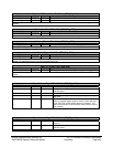
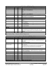
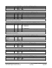
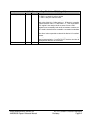
Input Phy Address and Data- R - 32 bits - [MEM_Reg: 10h]
Field Name Bits Default Description
Reserved 7:0 00h
Phy_in_read_flag 8 0h It is cleared whenever reg0x0Ch[8]=1 and reg0x0C[2]=1.
It is set when input physical data (due to a physical read) arrives.
in_Phy_addr 15:9 00h Physical address from AC'97 Codec.
Input Phy data 31:16 0000h Input Physical data from AC'97 Codec.
Input Phy address and data Register