


©2008 Advanced Micro Devices, Inc.
GPIO/GPOC
AMD SB600 Register Reference Manual Proprietary Page 277
4 Register Descriptions: General Purpose Functions/Interrupt
Controllers/Support Function Pins
4.1 GPIO/GPOC
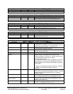
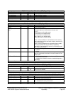
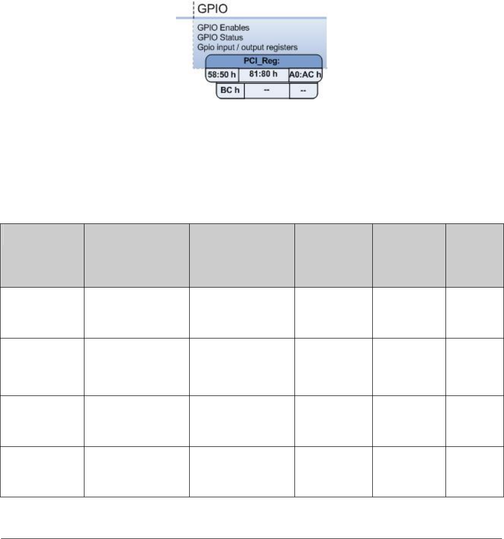
Note: Some GPIO functions are controlled by, and associated with, certain PCI configuration registers in the
SMBus/ACPI device. For more information refer to section 2.3: SMBus Module and ACPI Block (Device 20,
Function 0). The diagram below lists these GPIO functions and the associated registers.
4.1.1 GPIO
The GPIO pins, with the exception of GPIO0/2/10, cannot generate any events. The three lines of
GPIO0/2/10 can act either as GPIO lines or generate events. Refer to section 4.2.2 on how to program them
as event lines. The power-on default of the GPIO pins is GPI, but the BIOS can configure that to GPO.
Hardware strap can also enable the GPIO pins as dedicated functional pins if they are multi-functional pins.
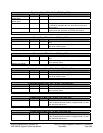
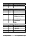
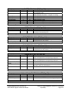
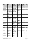
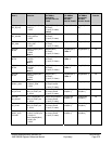
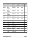
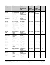
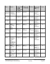
Table 4-1: GPIO Pins
Pin Name
(Note 1)
Multi-function
Selection
Output Enable
(On SMBus
Controller)
Bus 00h/ Dev14h/
Fun00
Input if GPI
(On SMBus
Controller)
Bus 00h/
Dev14h/ Fun00
Output if GPO
(On SMBus
Controller)
Bus 00h/
Dev14h/ Fun00
Power
Domain
GPIO0/
SSMUXSEL/
SATA_IS3#
PM IO Reg60h[Bit 7]
0: SSMUXSEL
1: GPIO if not used by
SATA
Reg80h[Bit 4]
0: Output
1: Input (Tri-state)
Reg81h[Bit 0] Reg80h[Bit 0] S0
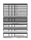
GPIO1/
ROM_CS#
If the chip is strapped
to use the ROM option
on the PCI bus, this
GPIO becomes
ROM_CS#
Reg80h[Bit 5]
0: Output
1: Input (Tri-state)
Reg81h[Bit 1] Reg80h[Bit 1] S0
GPIO2/
SPKR
PM IO Reg60h[Bit 5]
0: GPIO
1: SPKR
Reg80h[Bit 6]
0: Output
1: Input (Tri-state)
Reg81h[Bit 2]
Reg80h[Bit 2] S0
GPIO3/
FAN0
PM IO Reg60h[Bit 6]
0: GPIO
1: FAN0
Reg80h[Bit 7]
0: Output
1: Input (Tri-state)
Reg81h[Bit 3]
Reg80h[Bit 3] S0