


©2008 Advanced Micro Devices, Inc.
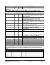
SMBus Module and ACPI Block (Device 20, Function 0)
AMD SB600 Register Reference Manual Proprietary Page 116
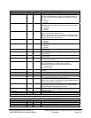
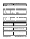
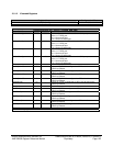
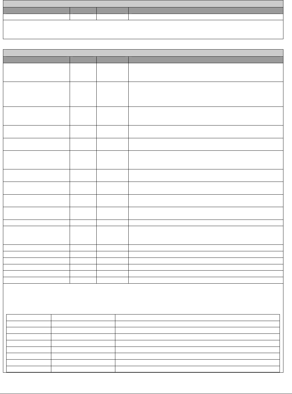
UsbIntMap - RW - 16 bits - [PCI_Reg: BEh]
Field Name Bits Default Description
Reserved 15:14 00b
UsbIntMap register
Encoding:
000 - INTA#, 001 - INTB#, 010 - INTC#, 011 - INTD#, 100 - INTE#, 101 - INTF#, 110 - INTG#, 111 - INTH#
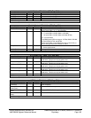
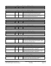
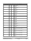
IoDrvSth - RW - 32 bits - [PCI_Reg: C0h]
Field Name Bits Default Description
IoDrvSth_AD 1:0 11b IO drive strength (bits [2:1]); together with bit 26 make up the
drive strength control for AD[31:0], CBE0#, CBE1#, CBE2#,
CBE3# and PAR pads.
IoDrvSth_Cntrl 3:2 11b IO drive strength (bits [2:1]); together with bit 26 make up the
drive strength control for A_RST#, FRAME#, IRDY#,
DEVSEL#, TRDY#, LOCK#, STOP#, PERR#, SERR#,
CLKRUN# and PCIRST# pads
IoDrvSth_GNT 5:4 11b IO drive strength (bits [2:1];; together with bit 27 make up the
drive strength control for GNT#[2:0], GNT3#, GNT4#, GNT5#,
and GNT6# pads
IoDrvSth_ClkGrpA 7:6 11b IO drive strength (bits [2:1];; together with bit 27 make up the
drive strength control for PCICLK[6:5] pads
IoDrvSth_ClkGrpB 9:8 11b IO drive strength (bits [2:1];; together with bit 27 make up the
drive strength control for PCICLK[4:1] pads
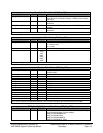
IoDrvSth_Lpc 12:11 11b IO drive strength (bits [2:1];; together with bit 28 make up the
drive strength control for LAD[3:0], LFRAME#, and
LDRQ#[1:0] pads
IoDrvSth_Ac97 13:12 11b IO drive strength for AC_SYNC, AC_SDOUT and SPDIF_OUT
pads
IoDrvSth_Int 15:14 11b IO drive strength for INTA#, INTB#, INTC#, INTD#, INTE#,
INTF#, INTG# and INTH# pads
IoDrvSth_Req 17:16 11b IO drive strength for REQ#[1:0], REQ3#, REQ4#, REQ5# and
REQ6# pads when these pads are configured as GPIO
IoDrvSth_GpioA 19:18 11b IO drive strength for BMREQ#, EXTEVENT1#, GPIO[0, 1, 2, 4,
5, 6, 7, 8, 9, 10, 13, 37], GPOC[0:1], DPRSLPVR,
IoDrvSth_GpioB 21:20 IO drive strength for GPIO[3, 48:52],
IoDrvSth_Misc 23:22 11b IO drive strength (bits [2:1];; together with bit 29 make up the
drive strength control for CPU_STP#/DPSLP_3V#, GA20IN,
KBRST#, SERIRQ and SATA_ACT# pads
IoDrvSth_Ide 25:24 11b IO drive strength for IDE pads
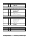
IoDrvSth_AD_0 26 1b Bit 0 of IoDrvSth_AD
IoDrvSth_GNT_0 27 1b Bit 0 of IoDrvSth_GNT
IoDrvSth_Lpc_0 28 1b Bit 0 of IoDrvSth_Lpc
IoDrvSth_Misc_0 29 1b Bit 0 of IoDrvSth_Misc
Reserved 31:30 11b
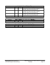
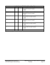
IoDrvSth: Each three bit field controls the number of P and N transistors enabled in the final stage of the output
driver for the designated pads. By controlling the number of transistors enabled, the designer can optimize the drive
characteristics of signals based on the topology of their specific design. For drive strength with 3 bit control, the
drive strength table is shown below. The values are non-linear and values for each bit field of this register are as
follows:
Value Relative Strength Description
111b 100% All P and N transistors are enabled when the pad drives
110b 88% Approximately 88% of the P and N transistors are enabled
101b 77% Approximately 77% of the P and N transistors are enabled
100b 66% Approximately 66% of the P and N transistors are enabled
011b 66% Approximately 66% of the P and N transistors are enabled
010b 55% Approximately 55% of the P and N transistors are enabled
001b 44% Approximately 44% of the P and N transistors are enabled
000b 33% Approximately 33% of the P and N transistors are enabled