


©2008 Advanced Micro Devices, Inc.
AC ’97 Controller Functional Descriptions
AMD SB600 Register Reference Manual Proprietary Page 217
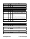
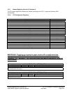
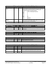
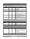
MSI Message Control Register- RW - 16 bits - [PCI_Reg: 42h]
Field Name Bits Default Description
Multiple Message
Enable
6:4 0b Software programs a 3-bit value into this field indicating the
actual number of messages allocated to the device. The number
allocated can be equal or less than the number actually
requested. The field is encoded as follows:
Value Number of Messages Requested
000b 1
001b 2
010b 4
011b 8
100b 16
101b 32
110b Reserved
111b Reserved
64-bit Address
Capable
7 0b Hardwired to 0 to indicates that function does not implement the
upper 32 bits of the Message Address register and is incapable
of generating a 64-bit memory address.
Reserved 15:8 00h
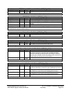
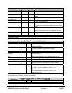
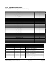
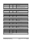
MSI Message Address Register- RW – 32 bits - [PCI_Reg: 44h]
Field Name Bits Default Description
Reserved 1:0 Reserved.
MSI Address 31:2 0000_00
00h
Lower 32 bits of the system specified message address always
DW aligned.
MSI Message Data Register- RW – 16 bits - [PCI_Reg: 48h]
Field Name Bits Default Description
MSI Data 15:0 0h System-specified message.
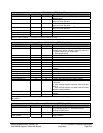
MSI Program Weight Register RW- 8 bits - [PCI_Reg: 4Ch]
Field Name Bits Default Description
MSI Program Weight 5:0 000100
b
This register specifies the programmable priority of modem device’s
message signaled interrupt request.
Reserved 7:6 0h
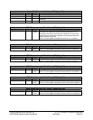
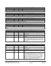
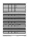
UnMask Latency Timer Expiration W - 32 bits - [PCI_Reg: 50h]
Field Name Bits Default Description
Reserved 0 0b
Base1Enable 1 0b When set, Base 1 (offset 14h) becomes writeable.
Reserved 2 0b
LargeMemEnable 3 0b When set, bits [13:8] of base 0 (offset 10h) becomes unwritable.
This is to cause OS to allocate wider memory map for ac97.
Reserved 31:4 0000_0
00h