


Intel
®
IXP42X Product Line of Network Processors and IXC1100 Control Plane Processor
September 2006 DM
Order Number: 252480-006US 165
Intel XScale
®
Processor—Intel
®
IXP42X product line and IXC1100 control plane processors
3.9.4.5 Saturated Arithmetic Instructions
h
3.9.4.6 Status Register Access Instructions
3.9.4.7 Load/Store Instructions
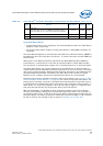
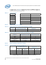
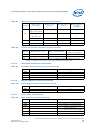
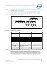
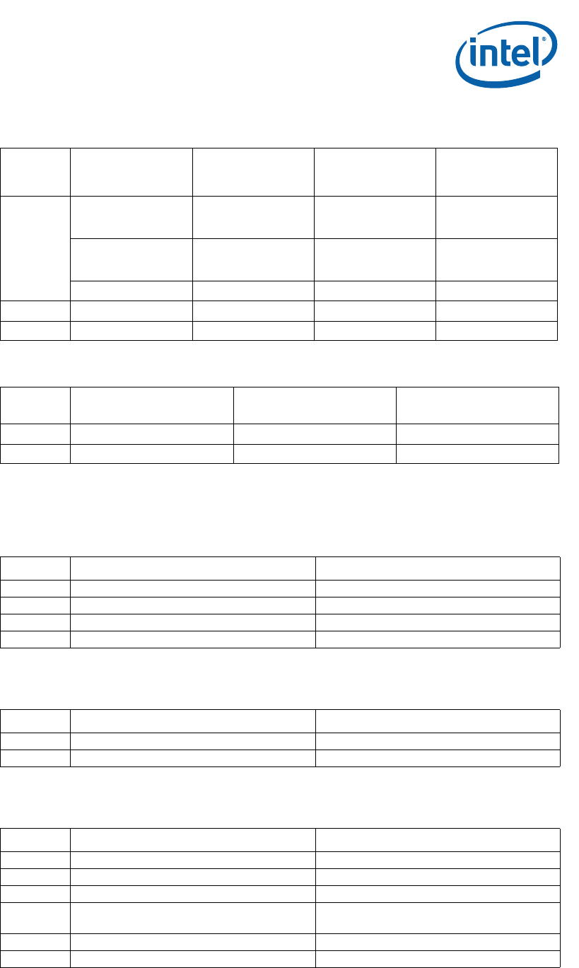
Table 82. Multiply Implicit Accumulate Instruction Timings
Mnemonic
Rs Value (Early
Termination)
Minimum Issue
Latency
Minimum Result
Latency
Minimum Resource
Latency
(Throughput)
MIA
Rs[31:15] = 0x0000
or
Rs[31:15] = 0xFFFF
111
Rs[31:27] = 0x0
or
Rs[31:27] = 0xF
122
all others 1 3 3
MIAxy N/A 1 1 1
MIAPH N/A 1 2 2
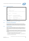
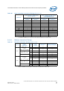
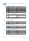
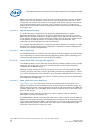
Table 83. Implicit Accumulator Access Instruction Timings
Mnemonic Minimum Issue Latency Minimum Result Latency
Minimum Resource
Latency (Throughput)
MAR 2 2 2
MRA 1 (RdLo = 2; RdHi = 3)
*
2
Note: If the next instruction needs to use the result of the MRA for a shift by immediate or as Rn in a
QDADD or QDSUB, one extra cycle of result latency is added to the number listed.
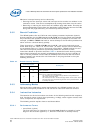
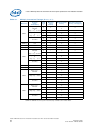
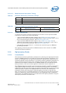
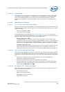
Table 84. Saturated Data Processing Instruction Timings
Mnemonic Minimum Issue Latency Minimum Result Latency
QADD 1 2
QSUB 1 2
QDADD 1 2
QDSUB 1 2
Table 85. Status Register Access Instruction Timings
Mnemonic Minimum Issue Latency Minimum Result Latency
MRS 1 2
MSR 2 (6 if updating mode bits) 1
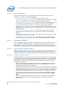
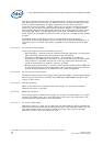
Table 86. Load and Store Instruction Timings
Mnemonic Minimum Issue Latency Minimum Result Latency
LDR 1 3 for load data; 1 for writeback of base
LDRB 1 3 for load data; 1 for writeback of base
LDRBT 1 3 for load data; 1 for writeback of base
LDRD 1 (+1 if Rd is R12)
3 for Rd; 4 for Rd+1;
1 (+1 if Rd is R12) for write-back of base
LDRH 1 3 for load data; 1 for writeback of base
LDRSB 1 3 for load data; 1 for writeback of base