Intel
®
IXP42X Product Line of Network Processors and IXC1100 Control Plane Processor
September 2006 DM
Order Number: 252480-006US 227
PCI Controller—Intel
®
IXP42X product line and IXC1100 control plane processors
The IXP42X product line and IXC1100 control plane processors will drive all the byte
enables asserted during all memory cycle reads of the external PCI device, no matter
what the PCI_NP_CBE register contains in the byte enable bits.
To read non-prefetch memory sub-DWORDS (8-bit or 16-bit), use I/O reads. If it is
necessary to use memory cycle reads of sub-DWORDS, a hardware resolution may be
required. Contact your Intel field application engineer if you require a hardware
resolution.
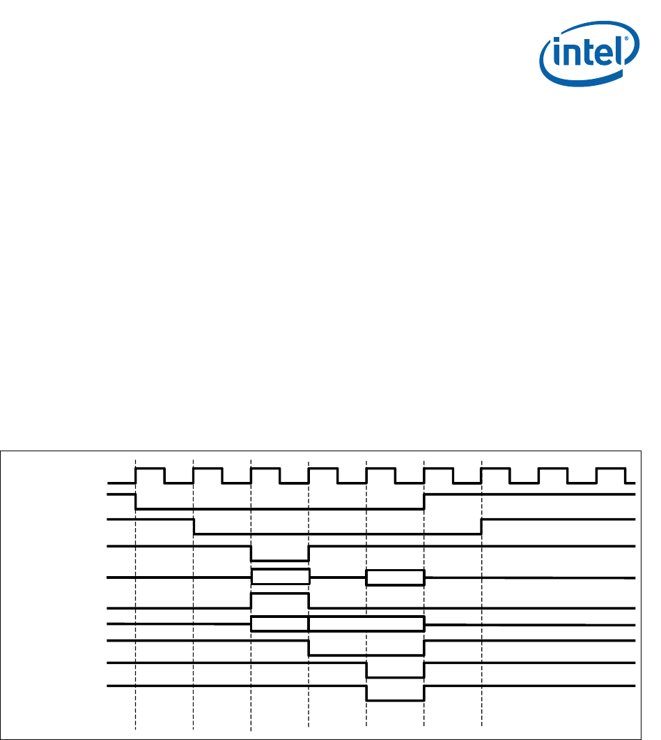
6.6.2 Initiated Type-0 Read Transaction
The following transaction is a PCI Configuration Read Cycle initiated from the IXP42X
product line and IXC1100 control plane processors. This diagram is to understand the
inner workings of PCI transfers and may not reflect actual operation of the PCI
Controller implemented on the IXP42X product line and IXC1100 control plane
processors. The Configuration transaction is initiated to the local PCI bus segment,
Device number (chosen by IDSEL), Function 0, and Base Address Register 0.
The IDSEL signal is left up to the user to determine how to drive this signal. It may be
driven from one of the upper address signals on the PCI_AD bus. A hexadecimal value
of 0xA, written on the PCI_C/BE_N bus during the PCI Bus address phase, signifies that
this is a PCI Bus Configuration Read Cycle.
6.6.3 Initiated Type-0 Write Transaction
The following transaction is a PCI Configuration Write Cycle initiated from the IXP42X
product line and IXC1100 control plane processors. This diagram is to understand the
inner workings of PCI transfers and may not reflect actual operation of the PCI
Controller implemented on the IXP42X product line and IXC1100 control plane
processors. The transaction is initiated to the local PCI bus segment, Device number
(chosen by IDSEL), Function number 2, and Base Address Register 0.
The IDSEL signal is left up to the user to determine how to drive this signal. It may be
driven from one of the upper address signals on the PCI_AD bus. A hexadecimal value
of 0xB written on the PCI_C/BE_N bus — during the address phase — signifies that this
is a PCI Bus Configuration Write Cycle.
Figure 35. Initiated PCI TYPE 0 Configuration Read Cycle
PCI_CLK
PCI_FRAME_N
PCI_AD (31:0)
PCI_IDSEL
PCI_C/BE_N
PCI_IRDY_N
PCI_TRDY_N
PCI_DEVSEL_N
0x00000010
DATA
0xA 0x0
INT_REQ_N
INT_GNT_N


