


Intel
®
IXP42X product line and IXC1100 control plane processors—PCI Controller
Intel
®
IXP42X Product Line of Network Processors and IXC1100 Control Plane Processor
DM September 2006
248 Order Number: 252480-006US
6.12 PCI Controller Clock and Reset Generation
The PCI Reset and PCI clock signals can be provided using general-purpose input/
output (GPIO) outputs or from an external source. GPIO 14 can be used to source up to
a 33-MHz clock output that can be used as the PCI Clock input to the chip and other PCI
Devices.
One of GPIO 13:0 can be used to generate the PCI Reset. Both signals can be sourced
from an external device as well. The Intel XScale processor can generate the PCI reset
and PCI clock outputs to satisfy the reset timing requirements of the PCI bus.
A PCI startup sequence could be as follows:
1. Power-on reset occurs to the IXP42X product line and IXC1100 control plane
processors, the Intel XScale processor starts execution (internal PLL assumed
locked and internal clocks stable).
2. Software configures PCI reset and PCI clock GPIOs as outputs driving 0. A pull-
down on the GPIO pin chosen to drive the PCI reset signal is required. This pull-
down is required because the GPIO are at a tristated value until the device comes
completely out of reset and the PCI reset needs to be low from the start.
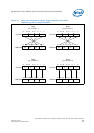
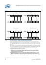
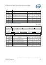
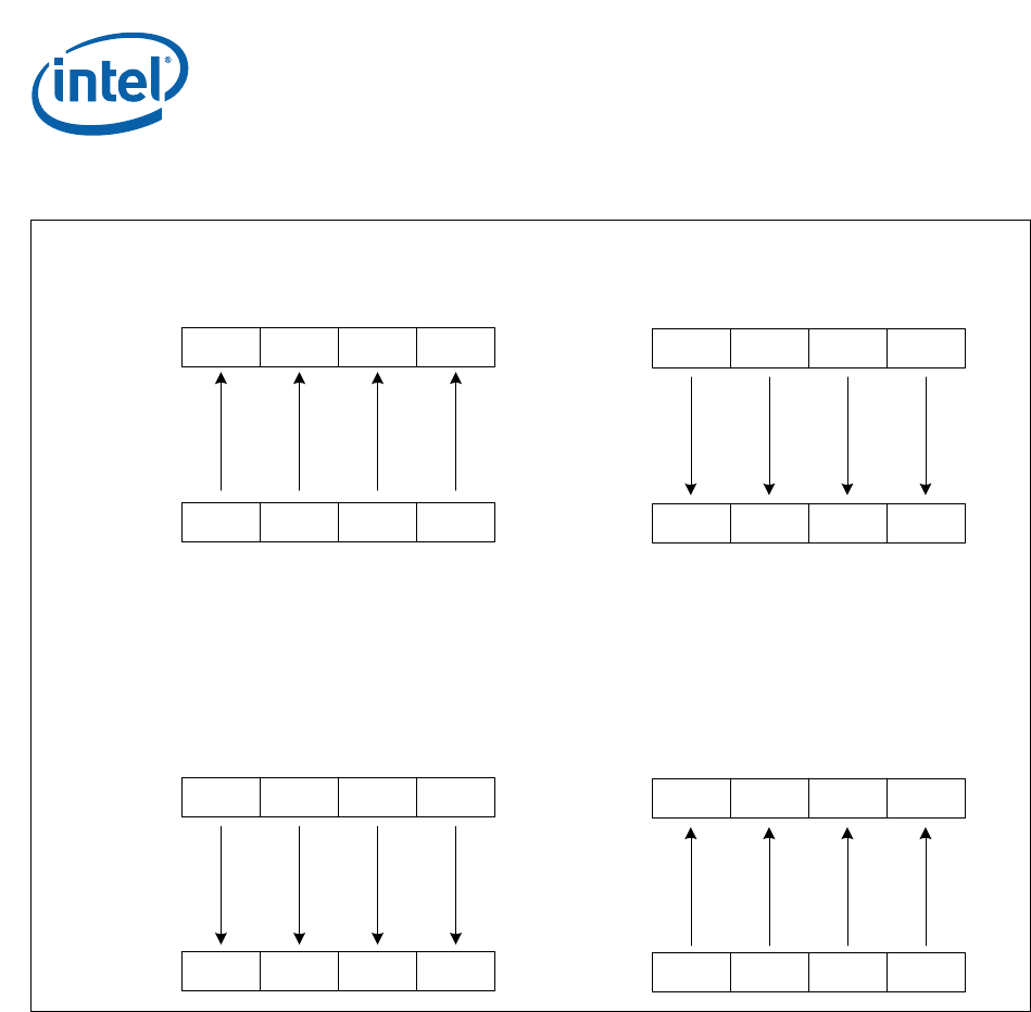
Figure 52. Byte Lane Routing During Configuration and Status Register Accesses
31
24
PCI CSR Read
CSR
Register
3
2
1
0
23
16
15
8
7
0
31
24
23
16
15
8
7
0
31
24
3 2
1
0
23
16
15
8
7
0
31
24
23
16
15
8
7
0
CSR
Register
PCI Data PCI Data
PCI CSR Write
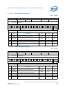
31
24
AHB CSR Read
AHB Data
23
16
15
8
7
0
31
24
23
16
15
8
7
0
31
24
23
16
15
8
7
0
31
24
23
16
15
8
7
0
AHB Data
CSR
Register
CSR
Register
AHB CSR Write