Intel
®
IXP42X Product Line of Network Processors and IXC1100 Control Plane Processor
September 2006 DM
Order Number: 252480-006US 215
PCI Controller—Intel
®
IXP42X product line and IXC1100 control plane processors
Configuration cycles will be produced by the IXP42X product line and IXC1100 control
plane processors using four 32-bit Configuration and Status Registers referred to as the
Non-Pre-fetch Registers. These registers are
• PCI Non-Pre-fetch Access Address (PCI_NP_AD) Register
• PCI Non-Pre-fetch Access Command/Byte Enables (PCI_NP_CBE) Register
• PCI Non-Pre-fetch Access Write Data (PCI_NP_WDATA) Register
• PCI Non-Pre-fetch Access Read Data (PCI_NP_RDATA) Register
The Non-Pre-fetch Register accesses can also be used to produce memory and I/O PCI
bus cycle. However, these cycles can only be single cycle accesses.
Non-Pre-fetch Read Cycles will be implemented by placing a 32-bit PCI address in the
PCI Non-Pre-fetch Access Address (PCI_NP_AD) Register and then placing the PCI
Command Type and Byte Enables for the desired read cycle in the PCI Non-Pre-fetch
Access Command/Byte Enables (PCI_NP_CBE) Register. The PCI Controller then will
initiate the proper transaction on the PCI bus to read the requested data. Then the
returned data is placed in the PCI Non-Pre-fetch Access Read Data (PCI_NP_RDATA)
Register.
To avoid incorrect data from being read by the initiator of this transaction, retries will
be issued to any AHB master that attempts to read the PCI Controller Configuration and
Status Registers prior to the Non-Pre-fetch PCI read data being placed into the PCI
Non-Pre-fetch Access Read Data (PCI_NP_RDATA) Register. This action assures that the
next read of the PCI Non-Pre-fetch Access Read Data (PCI_NP_RDATA) Register does
not contain stale data.
Non-Pre-fetch Write Cycles will be implemented by:
• Placing a 32-bit PCI address in the PCI Non-Pre-fetch Access Address (PCI_NP_AD)
Register
• Placing the PCI Command Type and Byte Enables for the desired write cycle in the
PCI Non-Pre-fetch Access Command/Byte Enables (PCI_NP_CBE) Register
• Writing the data that is to be placed onto the PCI bus into the PCI Non-Pre-fetch
Access Write Data (PCI_NP_WDATA) Register
The PCI Controller then will initiate the proper transaction on the PCI bus to place the
requested write data onto the PCI bus. To avoid the write data from being corrupted by
new request from an AHB master, retries will be issued to any AHB master that
attempts to write the PCI Controller Configuration and Status Registers prior to the
completion of the requested PCI transaction.
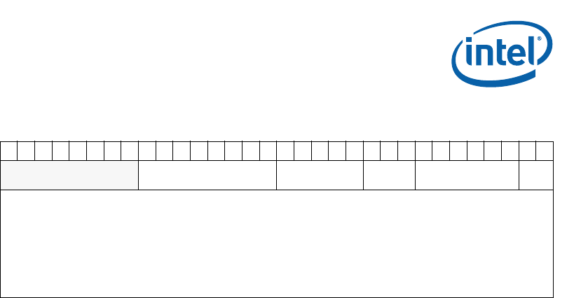
Figure 34. Type 1 Configuration Address Phase
31
24
23
16
15
11
10
8
7
2
1
0
(Reserved) Bus Segment Number Device Number
Function
Number
Register Number
Cycle
Type
Cycle Type =01 for Type 1 Configuration Cycles
Register Number =Defines one of 64 PCI defined 32-bit registers
Function Number=Decodes one of eight possible functions per PCI device (only Function 0 supported for the
IXP42X product line and IXC1100 control plane processors)
Device Number =Decodes one of 32 possible devices per PCI bus segment (may be limited by loading
restrictions, refer to the PCI Local Bus Specification, Rev. 2.2)
Bus Segment Number = Decodes one of 256 possible bus segments per PCI Bus (refer to the PCI Local Bus
Specification, Rev. 2.2)


