Intel
®
IXP42X product line and IXC1100 control plane processors—Intel XScale
®
Processor
Intel
®
IXP42X Product Line of Network Processors and IXC1100 Control Plane Processor
DM September 2006
72 Order Number: 252480-006US
Tags can be locked into the data cache by enabling the data cache lock mode bit
located in coprocessor 15, register 9. (See Table 20, “Cache Lock-Down Functions” on
page 83 for the exact command.) Once enabled, any new lines allocated into the data
cache will be locked down.
Note that the PLD instruction will not affect the cache contents if it encounters an error
while executing. For this reason, system software should ensure the memory address
used in the PLD is correct. If this cannot be ascertained, replace the PLD with a LDR
instruction that targets a scratch register.
Lines are locked into a set starting at way0 and may progress up to way 27; which set
a line gets locked into depends on the set index of the virtual address of the request.
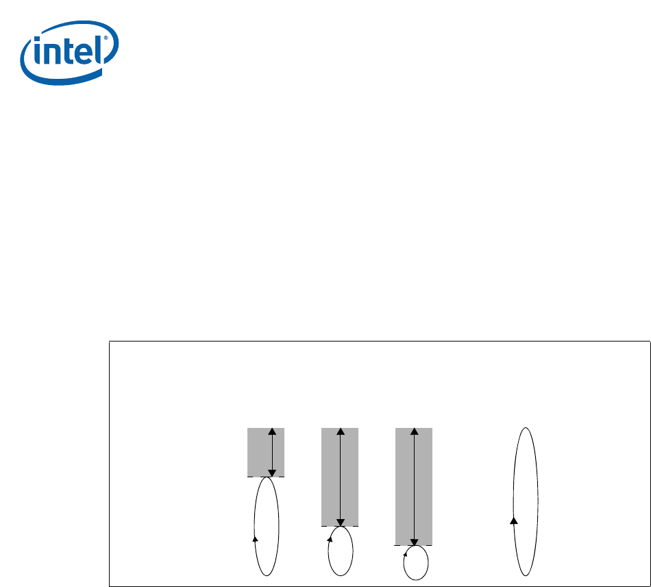
Figure 9, “Locked Line Effect on Round-Robin Replacement” on page 57 is an example
of where lines of code may be locked into the cache along with how the round-robin
pointer is affected.
Software can lock down data located at different memory locations. This may cause
some sets to have more locked lines than others as shown in Figure 9.
Lines are unlocked in the data cache by performing an unlock operation. See “Register
9: Cache Lock Down” on page 82 for more information about locking and unlocking the
data cache.
Before locking, the programmer must ensure that no part of the target data range is
already resident in the cache. The Intel XScale processor will not refetch such data,
which will result in it not being locked into the cache. If there is any doubt as to the
location of the targeted memory data, the cache should be cleaned and invalidated to
prevent this scenario. If the cache contains a locked region which the programmer
wishes to lock again, then the cache must be unlocked before being cleaned and
invalidated.
See “Terminology and Conventions” on page 26 for a definition of coalescing.
The write buffer is always enabled which means stores to external memory will be
buffered. The K bit in the Auxiliary Control Register (CP15, register 1) is a global
enable/disable for allowing coalescing in the write buffer. When this bit disables
coalescing, no coalescing will occur regardless the value of the page attributes. If this
bit enables coalescing, the page attributes X, C, and B are examined to see if
coalescing is enabled for each region of memory.
Figure 14. Locked Line Effect on Round-Robin Replacement
way 0
way 1
way 7
way 8
way 22
way 23
way 30
way 31
set 1
set 31
Locked
set 0
Locked
set 2
Locked
...
...
......
set 0: 8 ways locked, 24 ways available for round robin replacement
set 1: 23 ways locked, 9 ways available for round robin replacement
set 2: 28 ways locked, only ways 28-31 available for replacement
set 31: all 32 ways available for round robin replacement


