10-2 March, 2003 Developer’s Manual
Intel
®
80200 Processor based on Intel
®
XScale
™
Microarchitecture
External Bus
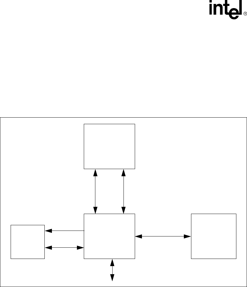
An alternate configuration with a separate memory bus is also possible, shown in Figure 10-2. All
signals on this bus, data and request, are sampled on the rising edge of MCLK. MCLK is created
by the system and is an input to the Intel
®
80200 processor. MCLK is asynchronous with respect
to the Intel
®
80200 processor core frequency and any other Intel
®
80200 processor input clocks.
MCLK in the configuration shown in Figure 10-1 would also need to be the SDRAM clock.
MCLK frequencies of up to 100 MHz are supported. A 50% duty cycle is required. MCLK must
be one third or less of the internal clock frequency of the core, however. An Intel
®
80200 processor
system running the core at 200 MHz would be allowed a maximum MCLK of 66 MHz, for
example. This constraint comes from the design of the low latency synchronization logic in the
Intel
®
80200 processor bus controller.
Figure 10-2. Alternate Configuration
SDRAM
ROM/
Flash
Chipset
Request
Data
Adr/Ctl
Data
PCI
Memory Bus
Intel
®
80200
Processor
based on
Intel® XScale™
Microarchitecture


