13-26 March, 2003 Developer’s Manual
Intel
®
80200 Processor based on Intel
®
XScale
™
Microarchitecture
Software Debug
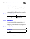
13.12 Trace Buffer
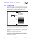
The 256 entry trace buffer provides the ability to capture control flow information to be used for
debugging an application. Two modes are supported:
1. The buffer fills up completely and generates a debug exception. Then SW empties the buffer.
2. The buffer fills up and wraps around until it is disabled. Then SW empties the buffer.
13.12.1 Trace Buffer CP Registers
CP14 defines three registers (see Table 13-14) for use with the trace buffer. These CP14 registers
are accessible using MRC, MCR, LDC and STC (CDP to any CP14 registers causes an undefined
instruction trap). The CRn field specifies the number of the register to access. The CRm, opcode_1,
and opcode_2 fields are not used and should be set to 0.
Any access to the trace buffer registers in User mode causes an undefined instruction exception.
Specifying registers which do not exist has unpredictable results.
13.12.1.1 Checkpoint Registers
When the debugger reconstructs a trace history, it is required to start at the oldest trace buffer entry
and construct a trace going forward. In fill-once mode and wrap-around mode when the buffer does
not wrap around, the trace can be reconstructed by starting from the point in the code where the
trace buffer was first enabled.
The difficulty occurs in wrap-around mode when the trace buffer wraps around at least once. In this
case the debugger gets a snapshot of the last N control flow changes in the program, where N <=
size of buffer. The debugger does not know the starting address of the oldest entry read from the
trace buffer. The checkpoint registers provide reference addresses to help reduce this problem.
The two checkpoint registers (CHKPT0, CHKPT1) on the Intel
®
80200 processor provide the
debugger with two reference addresses to use for re-constructing the trace history.
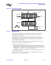
Table 13-14. CP 14 Trace Buffer Register Summary
CP14 Register Number Register Name
11 Trace Buffer Register (TBREG)
12 Checkpoint 0 Register (CHKPT0)
13 Checkpoint 1 Register (CHKPT1)
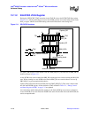
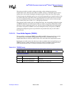
Table 13-15. Checkpoint Register (CHKPTx)
31 30 29 28 27 26 25 24 23 22 21 20 19 18 17 16 15 14 13 12 11 10 9 8 7 6 5 4 3 2 1 0
CHKPTx
reset value: Unpredictable
Bits Access Description
31:0 Read/Write
CHKPTx:
target address for corresponding entry in trace buffer


