Developer’s Manual March, 2003 7-7
Intel
®
80200 Processor based on Intel
®
XScale
™
Microarchitecture
Configuration
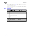
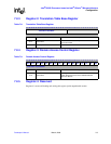
7.2.2 Register 1: Control and Auxiliary Control Registers
Register 1 is made up of two registers, one that is compliant with ARM Version 5 and is referenced
by opcode_2 = 0x0, and the other which is specific to Intel
®
StrongARM* and is referenced by
opcode_2 = 0x1.
The Exception Vector Relocation bit (bit 13 of the ARM control register) allows the vectors to be
mapped into high memory rather than their default location at address 0. This bit is readable and
writable by software. If the MMU is enabled, the exception vectors are accessed via the usual
translation method involving the PID register (see Section 7.2.13, “Register 13: Process ID” on
page 7-16) and the TLBs. To avoid automatic application of the PID to exception vector accesses,
software may relocate the exceptions to high memory.
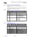
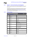
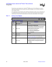
Table 7-6. ARM* Control Register
31 30 29 28 27 26 25 24 23 22 21 20 19 18 17 16 15 14 13 12 11 10 9 8 7 6 5 4 3 2 1 0
V I Z0RSB11 11CAM
reset value: writeable bits set to 0
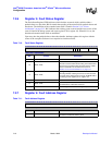
Bits Access Description
31:14
Read-Unpredictable /
Write-as-Zero
Reserved
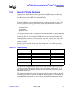
13 Read / Write
Exception Vector Relocation (V).
0 = Base address of exception vectors is 0x0000,0000
1 = Base address of exception vectors is 0xFFFF,0000
12 Read / Write
Instruction Cache Enable/Disable (I)
0 = Disabled
1 = Enabled
11 Read / Write
Branch Target Buffer Enable (Z)
0 = Disabled
1 = Enabled
10 Read-as-Zero / Write-as-Zero Reserved
9 Read / Write
ROM Protection (R)
This selects the access checks performed by the memory
management unit. See the
ARM Architecture Reference
Manual
for more information.
8 Read / Write
System Protection (S)
This selects the access checks performed by the memory
management unit. See the
ARM Architecture Reference
Manual
for more information.
7 Read / Write
Big/Little Endian (B)
0 = Little-endian operation
1 = Big-endian operation
6:3 Read-as-One / Write-as-One = 0b1111
2 Read / Write
Data cache enable/disable (C)
0 = Disabled
1 = Enabled
1 Read / Write
Alignment fault enable/disable (A)
0 = Disabled
1 = Enabled
0 Read / Write
Memory management unit enable/disable (M)
0 = Disabled
1 = Enabled


