Developer’s Manual March, 2003 C-1
Test Features C
The Intel
®
80200 processor based on Intel
®
XScale
™
microarchitecture (compliant with the
ARM* Architecture V5TE) implements Design For Test (DFT) techniques to ensure quality and
reliability. This appendix describes those techniques.
C.1 Introduction
Testing VLSI circuits is critical for achieving high outgoing quality levels. Unfortunately the cost
of testing is already one of the largest portions of the final product cost and is getting more
expensive as the complexity of VLSI chips grows. Reducing test cost is thus one of the critical
issues that must be resolved in order to make a cost competitive VLSI chip, and area and/or delay
minimization at the cost of increased test time may not be a good design choice.
Testability is the ability or ease with which tests can be generated for and applied to CUT (Circuit
Under Test). Design For Testability (DFT) stands for having design decisions early in the design
cycle that ease the testing, test generation, and fault grading process for a given circuit.
C.2 JTAG - IEEE1149.1
The goal of JTAG also known as IEEE1149.1 is to ensure that chips containing a common
denominator of DFT circuitry makes testing of boards containing these chips significantly less
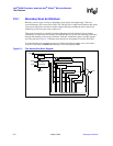
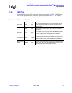
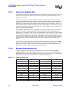
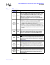
costly and more effective. JTAG consists of TAP controller, Boundary-Scan register, instruction
and data registers, and dedicated signals including TDI, TDO, TCK, TMS, and TRST#.
The Intel
®
80200 processor provides test features compatible with IEEE Standard Test Access Port
and Boundary Scan Architecture (IEEE Std. 1149.1). JTAG ensures that components function
correctly, connections between components are correct, and components interact correctly on the
printed circuit board.


