


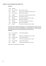

88
CHAPTER 3 CLOCK GENERATOR AND CONTROLLER
[Example]
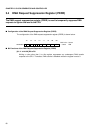
The output from the divide-by-two frequency circuit can be selected as the source clock by
setting the CHC bit of the gear control register to 1. Setting the CHC bit to 0 selects the clock
having the same cycle as the clock generated from the oscillation circuit. Since the source
clock is changed, the CPU and peripheral systems change simultaneously.
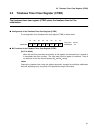
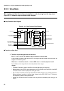
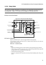
[Example]
Figure 3.9.2 is a timing chart for clock selection
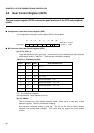
LDI:20 #GCR,R2
LDI:8 #11111110b,R1 ; CCK=11,PCK=11,CHC=0
STB R1.@R2 ; CPU clock=1/8f, Peripheral clock=1/8f, f=direct
LDI:8 #01111010b,R1 ; CCK=01,PCK=10,CHC=0
STB R1,@R2 ; CPU clock=1/2f, Peripheral clock=1/4f, f=direct
LDI:8 #00111010b,R1 ; CCK=00,PCK=10,CHC=0
STB R1,@R2 ; CPU clock=f, Peripheral clock=1/4f, f=direct
LDI:8 #00110010b,R1 ; CCK=00,PCK=00,CHC=0
STB R1,@R2 ; CPU clock=f, Peripheral clock=f, f=direct
LDI:8 #10110010b,R1 ; CCK=10,PCK=00,CHC=0
STB R1,@R2 ; CPU clock=1/4f, Peripheral clock=f, f=direct
LDI:8 #01110001b,R1 ; CCK=01,PCK=00,CHC=1
LDI:20 #GCR,R2
STB R1,@R2 ; CPU clock=1/2f, Peripheral clock=f, f=1/2xtal
LDI:8 #00110011b,R1 ; CCK=00,PCK=00,CHC=1
STB R1,@R2 ; CPU clock=f, Peripheral clock=f, f=1/2xtal
LDI:8 #00110010b,R1 ; CCK=00,PCK=00,CHC=0
STB R1,@R2 ; CPU clock=f, Peripheral clock=f, f=direct