


160
CHAPTER 4 BUS INTERFACE
❍
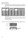
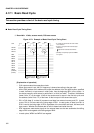
Usual DRAM interface
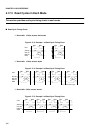
The usual DRAM interface converts the CAS cycle to a 2-clock cycle by setting the DSAS and
HYPR bits of DMCR4 and DCMR5 to "0". It handles "5-clock cycles" as basic bus cycles during
read and write operations. This manual represents these cycles as Q1 to Q5.
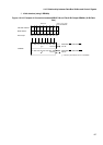
The high-speed page mode provides high-speed memory access using column addresses and
CAS control on the same page pace specified by the same row address. When using this
mode, set 1 in the PAGE bit of DMCR4 and DMCR5.
Whether access is within the same page is determined by the PGS3 to PGS0 bits of DMCR4
and DMCR5 as well as the bus width.
Access in the high-speed page mode starts when the usual access from the Q1 to Q5 cycle
ends. When the high-speed page mode is entered, the Q4 to Q5 cycles are repeated. Once
the page mode is entered, the RAS control signal remains at "L" unless a nonpage access or
refresh cycle occurs.
The Q1 and Q4 wait cycles can also be set in the high-speed page mode, where the Q4, Q4W,
and Q5 cycles are repeated.
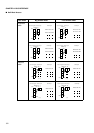
• Usual DRAM interface: Read
• Usual DRAM interface: Write
• Usual DRAM read cycle
• Usual DRAM write cycle
• Automatic wait cycle in usual DRAM interface
• DRAM interface in high-speed page mode
❍
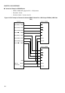
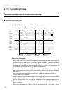
Single DRAM interface
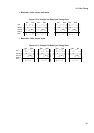
The single DRAM interface handles a CAS access as one clock cycle by setting "0" in the DSAS
bit of DMCR4 and DCMR5 and "1" in the HYPR bit. When using this mode, set "1" in the PAGE
bit of DMCR4 and DMCR5 to enable the high-speed page mode.
The single DRAM interface starts from the Q1 to Q2 cycle as with the usual DRAM interface.
When the Q4 cycle is entered, the CAS signal is controlled for one cycle and a read/write
operation is performed. This manual represents the Q4 cycle for a read operation by "Q4SR"
and by "Q4SW" for a write operation. Note that the page size, 1CAS/2WE and 2CAS/1WE
setting, and Q1 wait cycle are similar to those of the usual DRAM interface.
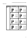
• Single DRAM interface: Read
• Single DRAM interface: Write
• Single DRAM interface
❍
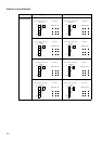
Hyper DRAM interface
The hyper DRAM interface handles a CAS access as one clock cycle and fetches an address
before data in a read cycle, thereby providing high-speed DRAM access by setting "1" in the
DSAS and HYPR bits of DMCR4 and DMCR5. Also, set "1" in the PAGE bit to enable the high-
speed page mode.
The hyper DRAM interface starts from the Q1 to Q3 cycle as with the usual DRAM interface.
When the Q4 cycle is entered, the CAS signal is controlled for one cycle and a read/write
operation is performed. This manual represents the Q4 cycle for a read operation by Q4HR and
Q4HW for a write operation. Note that the page size, 1CAS/2WE and 2CAS/1WE setting, and
Q1 wait cycle are similar to those of the usual DRAM interface.