


205
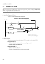
5.4 Using External Pins as I/O Ports
5.4 Using External Pins as I/O Ports
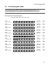
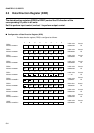
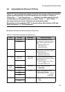
Table 5.4-1 lists the relationship between the initial value for each external pin and the
register specifying whether to use the external pin as an I/O port or control pin.
"Single chip: --- " and "External bus: --- " indicated in the table mean that the pin
function differs for the operation mode to be used. "8 bits: --- " and "16 bits: --- "
also mean that the pin function differs for each external bus width.
Pin numbers are the examples of QFP. As these numbers differ between LQFP and
FBGA, see Section 1.4, "Pin Assignments."
■
Selection of External Pin Function (I/O Port or Control Pin)
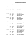
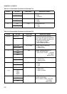
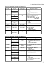
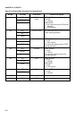
Table 5.4-1 External Bus Functions to be Selected (1/4)
Pin No. Pin code Initial value Switch-over register
28 to 35 P20 to P27 P20 to P27 Function automatically switches
according to the mode set by MD0 to
MD2, AMD0 to AMD5, and M0 to
M1.
Single chip: P20 to P27
8 bits: P20 toP27
16 bits: D16 to D23
D16 to D23
36 to 42, 44 P30 to P37 P30 to P37 Function automatically switches
according to the mode set by MD0 to
MD2 and M0 to M1.
Single chip: P30 to P37
External bus: D24 to D31
D24 to D31
45, 47 to 61 P40 to P47
P50 to P57
P40 to P47
P50 to P57
Function automatically switches
according to the mode set by MD0 to
MD2 and M0 to M1.
Single chip: P40 to P47, P50 to
P57
External bus: A00 to A15
A00 to A15
62 to 67,
69,70
P60 to P67 P60 to P67 EPCR1 (AE16 to AE23 bits)
0: P60 to P67
1: A16 to A23
A16 to A23
71 P70 P70 EPCR1 (AE24 bit) and DATCR
(EPSE0 and EPDE0 bits)
AE24, EPSE0, EPDE0 000:P70
100: A24
Others:E0P0
A24
EOP0
22 P80 P80 EPCR0 (RDYE bit)
0: P80
1: RDY
RDY