


127
4.10 DRAM Control Register 4/5 (DMCR4/5)
4.10 DRAM Control Register 4/5 (DMCR4/5)
DRAM control registers 4 and 5 (DMCR4 and DMCR5) control the DRAM interface for
areas 4 and 5 and are valid only when the DRME bits of AMD4 and AMD5 are set to "1".
■
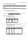
Configuration of DRAM Control Register 4/5 (DMCR4/5)
DRAM control register 4/5 are configured as follows:
■
Bit Functions of DRAM Control Register 4/5 (DMCR4/5)
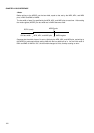
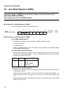
[bit 15 to 12] PGS 3 to 0 (PaGe size Select bit)
PGS3 to PGS0 specify the page size of the DRAM to be connected (see Table 4.10.1).
The bus interface unit determines the row size (page size) by the values of PGS3 to PGS0
as well as the specified bus width. If an intrapage access occurs when the register allows a
page access mode, a high-speed page access is executed.
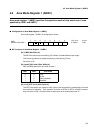
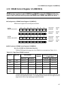
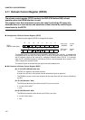
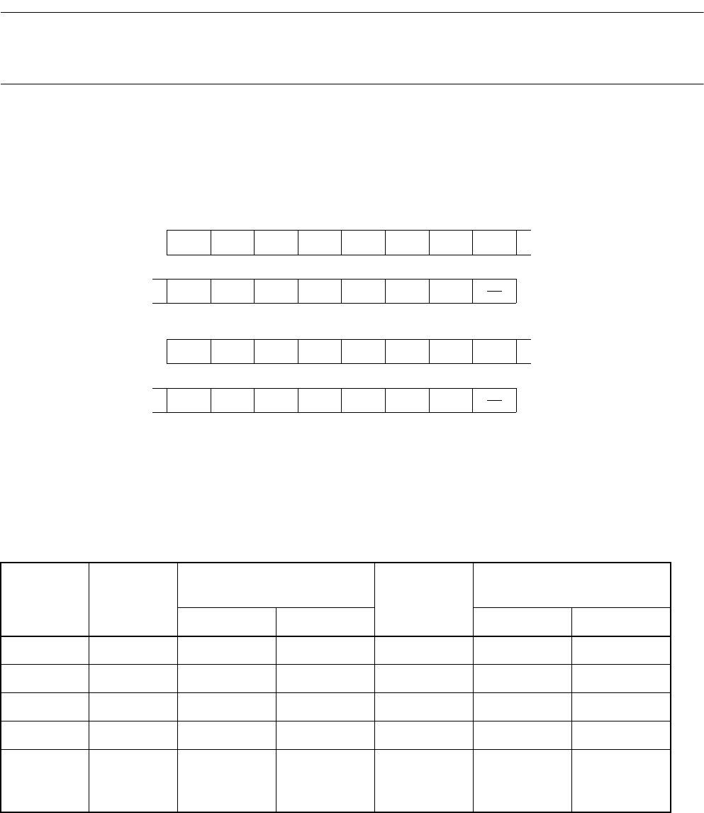
15 14 13 12 11 10 9 8
DMCR4
Address: 0000 062C
H
PGS3 PGS2 PGS1 PGS0 Q1W Q4W DSAS HYPR 00000000 R/W
76543210
PAG E C/W SLFR REFE PAR PERR PEIE 0000000- R/W
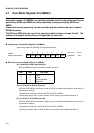
15 14 13 12 11 10 9 8
DMCR5
Address: 0000 062E
H
PGS3 PGS2 PGS1 PGS0 Q1W Q4W DSAS HYPR 00000000 R/W
76543210
PAG E C/W SLFR REFE PAR PERR PEIE 0000000- R/W
initial value
initial value
initial value
initial value
access
access
access
access
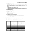
Table 4.10-1 Page Size of DRAM Connected
PGS3 to 0 Page size ROW Address Column
address
Determine whether access
is within page
A31 to 16 A15 to 00 8-bit bus 16-bit bus
0000 256 A31 to 16 A23 to 08 A31 to 00 A31 to 08 A31 to 09
0001 512 A31 to 16 A24 to 09 A31 to 00 A31 to 09 A31 to 10
0010 1024 A31 to 16 A25 to 10 A31 to 00 A31 to 10 A31 to 11
0011 4096 A31 to 16 A27 to 12 A31 to 00 A31 to 12 A31 to 13
0100
to
1111
reserved